
2-Channel I2C-UART 3.3V 5V Bi-Directional Logic Level Shifter Module (MD1055) Products
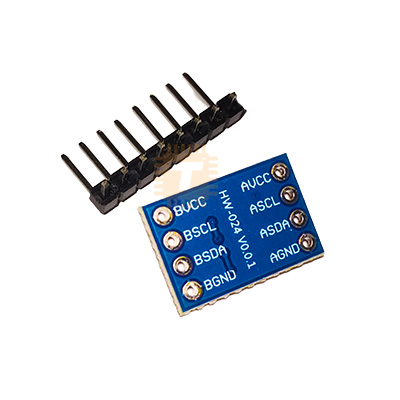
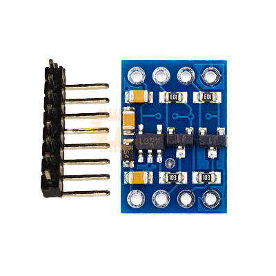
| Name | 2-Channel I2C-UART 3.3V 5V Bi-Directional Logic Level Shifter Module |
| Code | MD1055 |
| Price | Rs.60.00 |
| In Stock | Yes |
| Package | MODULE |
Product Details
The 2-Channel I2C-UART 3.3V 5V Bi-Directional Logic Level Shifter Module is a compact, breadboard-friendly level translation board designed to bridge mixed-voltage digital signaling between low-voltage 3.3V devices and legacy 5V hardware safely. Built around discrete N-channel enhancement-mode MOSFET switching architecture with on-board pull-up resistor arrays, it provides true bidirectional level shifting on two independent channels without requiring explicit directional control pins. Capable of shifting open-drain and push-pull communication protocols, this module protects sensitive 3.3V microcontroller and sensor inputs from 5V overvoltage damage, making it indispensable for inter-device UART, I2C, SPI, and 1-Wire serial bus interfacing.
Specifications
- Module Type: 2-Channel Bidirectional Digital Logic Level Translator / Converter
- High-Voltage Side Supply (HV): 3.3 V to 5.5 V DC (Must match the higher system voltage logic rail)
- Low-Voltage Side Supply (LV): 1.8 V to 3.3 V DC (Must match the lower system voltage logic rail)
- Operating Voltage Rule: HV rail voltage must always remain strictly greater than or equal to LV rail voltage ($V_{HV} \ge V_{LV}$)
- Number of Logic Channels: 2 Independent Bidirectional Channels (e.g., SDA & SCL or TX & RX)
- Level Shifting Architecture: Discrete N-Channel MOSFETs with Integrated Gate-Bias Circuitry
- Pull-Up Resistors: 10 kΩ Integrated Pull-Up Resistors on both HV and LV channels to their respective supply rails
- Maximum Data Rate: Up to 400 kHz (Standard/Fast I2C mode); up to 1 Mbps to 2 Mbps for push-pull serial UART depending on cable capacitance
- Pin Pitch: Standard 2.54 mm (0.1 Inch) breadboard-compatible header spacing
- Pinout Configuration:
- High-Voltage Side: HV (High-Voltage Reference In), GND (Common Ground), HV1 (High-Voltage Channel 1), HV2 (High-Voltage Channel 2)
- Low-Voltage Side: LV (Low-Voltage Reference In), GND (Common Ground), LV1 (Low-Voltage Channel 1), LV2 (Low-Voltage Channel 2)
- Operating Temperature: -40°C to +85°C
- PCB Dimensions: Approx. 15.2 mm × 12.7 mm × 2.5 mm
- Net Weight: Approx. 1.5 g (Excluding pin headers)
Features
- True Bidirectional Auto-Sensing Translation: Internal MOSFET topology automatically passes signals in either direction (HV → LV and LV → HV) without the need for direction-select control pins.
- I2C Bus Native Support: Built-in 10kΩ pull-up resistors on both high and low sides fully support open-drain bidirectional protocols such as I2C and SMBus out of the box.
- Overvoltage Input Clamping & Protection: Safely decouples 5V digital logic levels, ensuring sensitive 3.3V or 1.8V processing chips are never exposed to damaging overvoltage conditions.
- Breadboard-Friendly Footprint: Dual single-row 2.54mm pin spacing straddles standard prototyping breadboard center troughs with room for hookup jumpers on either side.
- Low Standby Power Drain: High-impedance pull-up networks and low-leakage MOSFET switches result in minimal parasitic power dissipation across idle lines.
Common Applications
- I2C Sensor Interfacing: Connecting 3.3V I2C digital sensors (accelerometers, gyroscopes, barometric pressure, RTCs) to 5V Arduino Uno/Mega boards without blowing input gates.
- UART Serial Communication: Interfacing 3.3V UART devices (ESP8266, ESP32, Raspberry Pi GPIO, Bluetooth HC-05/06 modules, GPS units) with 5V microcontroller serial ports.
- Microcontroller Cross-Communication: Safely linking 3.3V ARM Cortex-M / STM32 / RP2040 platforms to 5V peripheral modules, display controllers, and driver ICs.
- 1-Wire & Specialized Digital Busses: Bridging digital signals between mixed-supply components in home automation, smart agriculture, and IoT telemetry setups.
- DIY Prototyping & Breadboarding: Fast, dependable plug-in voltage isolation for maker benches, educational kits, and electronics hardware testing.
Usage Tips
- Power Connection Sequence (CRITICAL):
- Both HV and LV power pins must be connected to their respective system logic voltages. Connect 5V to the HV pin, connect 3.3V to the LV pin, and connect the circuit ground from both systems to the shared GND pins.
- The voltage connected to HV must always be higher than the voltage connected to LV. Powering LV with a higher voltage than HV will cause parasitic body diode conduction inside the MOSFETs, resulting in improper shifting and potential hardware damage.
- Common Ground Reference:
- Ensure the ground of the 5V host system and the 3.3V peripheral device share a common ground (GND) reference via the module's GND pins to maintain accurate logic thresholds.
- High-Speed SPI & Cable Capacitance Limitations:
- While excellent for I2C (up to 400 kHz) and standard baud rate UART (9600 to 115200 baud), this passive MOSFET-based shifter relies on 10kΩ pull-ups for logic rising edges.
- For high-speed SPI busses (>2 MHz to 10 MHz) or long capacitive cables, the RC time constant of the 10kΩ resistors will round off sharp square wave edges. If driving high-frequency lines, add external lower-value pull-ups (e.g., 2.2kΩ to 4.7kΩ) or use active push-pull IC level shifters (such as the 74LVC245 or TXS0108E).
- Channel Assignment: Each channel operates independently. For an I2C bus, wire SDA to LV1/HV1 and SCL to LV2/HV2. For UART communication, wire TX to LV1/HV1 and RX to LV2/HV2.
- Soldering Pin Headers: When attaching the included 2.54mm header pins, plug the pins directly into a solderless breadboard first to hold them perpendicular and parallel before soldering the PCB pads at 300°C to 330°C.
Sharing is caring, show love and share the product with your friends.
Featured

Add to Cart

Add to Cart


Add to Cart
Other Products


Add to Cart
