Original FDL100N50F 500V 100A N-Channel MOSFET TO-264 (DI0304) Products
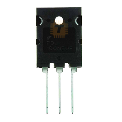
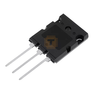
| Name | Original FDL100N50F 500V 100A N-Channel MOSFET TO-264 |
| Code | DI0304 |
| Price | Rs.4,200.00 |
| In Stock | Yes |
| Package | TO-264 |
Product Details
The Original FDL100N50F 500V 100A N-Channel Power MOSFET is an ultra-high-power planar DMOS transistor from the UniFET FRFET series by ON Semiconductor / Fairchild. Encapsulated in an extra-large, heavy-duty TO-264 through-hole package, this device features an exceptionally low on-state resistance (Rds(on)) of 43mΩ, massive continuous current carrying capacity of up to 100A, and an integrated fast-recovery body diode (FRFET) with low reverse recovery time (trr). Engineered for extreme power density, it is widely utilized in high-power uninterruptible power supplies (UPS), AC-DC industrial power converters, welding machines, plasma cutters, solar inverters, and active power factor correction (PFC) systems.
Specifications
- Part Number / Model: FDL100N50F (UniFET / FRFET Series / onsemi - Fairchild)
- Transistor Type: N-Channel Enhancement Mode Power MOSFET
- Package Type: TO-264
- Drain-Source Breakdown Voltage (Vds): 500V (at Tc = 25°C)
- Gate-Source Voltage (Vgs): ±30V
- Continuous Drain Current (Id):
- 100A (at Tc = 25°C)
- 60A (at Tc = 100°C)
- Pulsed Drain Current (Idm): 400A Peak
- Static Drain-Source On-Resistance (Rds(on)): Typ. 43mΩ / Max. 55mΩ (at Vgs = 10V, Id = 50A)
- Single Pulsed Avalanche Energy (Eas): 5000mJ (5.0 Joules, 100% Avalanche Tested)
- Body Diode Reverse Recovery Time (trr): Typ. 250ns (Fast Recovery FRFET)
- Gate Threshold Voltage (Vgs(th)): 3.0V to 5.0V (at Vds = Vgs, Id = 250µA)
- Total Gate Charge (Qg): Typ. 238nC (at Vds = 400V, Id = 50A, Vgs = 10V)
- Input Capacitance (Ciss): Typ. 12000pF (at Vds = 25V, f = 1MHz)
- Reverse Transfer Capacitance (Crss): Typ. 64pF
- Total Power Dissipation (Pd): Up to 2500W (Pulse peak rating) / Massive continuous thermal dissipation capacity
- Thermal Resistance, Junction to Case (Rth(j-c)): Max. 0.05°C/W (Ultra-Low Thermal Resistance)
- Operating Junction & Storage Temperature: -55°C to +150°C
- Pinout Configuration: Pin 1: Gate (G), Pin 2: Drain (D), Pin 3: Source (S), Tab: Drain (D)
Features
- Ultra-Low 43mΩ On-Resistance: Greatly reduces I²R conduction losses during heavy 50A–100A current delivery, maximizing overall electrical efficiency.
- Massive TO-264 Footprint & Rth(j-c) of 0.05°C/W: Provides an oversized thermal contact area with near-zero thermal resistance to metal heatsinks, allowing superior heat extraction compared to standard TO-247 packages.
- 5000mJ Avalanche Ruggedness: 100% avalanche tested to survive intense inductive kickback and transient energy spikes without device failure.
- Integrated Fast-Recovery Body Diode (FRFET): Enhanced lifetime-control body diode reduces reverse recovery losses and improves dv/dt ruggedness (20V/ns) in half-bridge and full-bridge bridge topologies.
- Low Reverse Transfer Capacitance (Crss = 64pF): Minimizes Miller effect capacitance, enabling clean, high-speed switching with reduced driver stress.
Common Applications
- High-Power Industrial Inverters & UPS: Main bridge switching stages for 5kVA to 20kVA+ online uninterruptible power supplies.
- Inverter Welders & Plasma Cutters: Primary high-current switching transistors for heavy-duty DC welding units.
- Active Power Factor Correction (PFC): Continuous Conduction Mode (CCM) boost converters in high-wattage power supplies.
- Solar & Wind Energy Converters: High-voltage DC-DC boost stages and central grid-tie inverters.
- High-Frequency Induction Heating: High-power full-bridge resonant tank drivers in metal hardening and melting systems.
Usage Tips
- Heavy-Duty Gate Driver Required: Due to the large input capacitance (~12000pF) and 238nC gate charge, always drive this MOSFET with a high-current gate driver (such as TC4420, TC4422, or IXDD614 providing 6A to 14A peak drive current) to achieve fast rise times and prevent thermal transition losses.
- Heatsink Mounting & Insulators: Mount the large TO-264 tab to a heavy, machined copper or aluminum heatsink using a matching oversized silicone thermal pad (TO-3P3 / TO-30 size) and high-temperature thermal compound.
- Lead Reinforcement & Busbars: When handling 50A to 100A continuous currents, solder heavy solid copper busbars directly along the source and drain PCB traces to avoid trace burn-out.
- Gate Ringing Suppression: Place a 2.2Ω to 10Ω non-inductive series gate resistor directly at Pin 1 (Gate) and use twisted pair or tight co-planar PCB routing from the gate driver.
Sharing is caring, show love and share the product with your friends.
Featured


Add to Cart

Add to Cart