Original IRFPS40N50L 500V 46A N-Channel Power MOSFET TO-247 (DI0317) Products
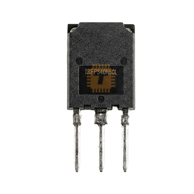
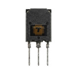
| Name | Original IRFPS40N50L 500V 46A N-Channel Power MOSFET TO-247 |
| Code | DI0317 |
| Price | Rs.2,780.00 |
| In Stock | Yes |
| Package | TO-252 (D-Pak) |
Product Details
The Original IRFPS40N50L 500V 46A N-Channel Power MOSFET (TO-247) is a high-voltage, high-current HEXFET power MOSFET designed for high-efficiency switch-mode power conversion, zero-voltage switching (ZVS) topologies, and high-frequency power applications. Featuring an ultra-low on-state resistance (RDS(on) typ. 0.087Ω / max. 0.100Ω) combined with an integrated superfast body diode, it delivers outstanding switching speed, low reverse recovery charge, and minimal conduction losses. Housed in the heavy-duty clip-mounted Super-247 (TO-274AA / TO-247 profile) through-hole power package, it is capable of dissipating up to 540W with an avalanche current rating of 46A. The IRFPS40N50L is widely utilized in high-power telecom and server SMPS, uninterruptible power supplies (UPS), solar string inverters, induction heating systems, active PFC boost stages, and industrial motor drives.
Specifications
- Part Number: IRFPS40N50L
- Transistor Polarity: N-Channel Enhancement Mode Power MOSFET
- Package Type: TO-274
- Drain-Source Breakdown Voltage (VDSS): 500 V (Min. at VGS = 0V, ID = 250µA)
- Gate-Source Voltage (VGS): ±30 V Max.
- Continuous Drain Current (ID):
- At TC = 25°C: 46 A (at VGS = 10V)
- At TC = 100°C: 29 A
- Pulsed Drain Current (IDM): Up to 180 A (Pulse width limited by max Tj)
- Static Drain-Source On-State Resistance (RDS(on)):
- Typ. 0.087 Ω (at VGS = 10V, ID = 28A)
- Max. 0.100 Ω (at VGS = 10V, ID = 28A)
- Gate Threshold Voltage (VGS(th)): 3.0 V to 5.0 V (at VDS = VGS, ID = 250µA)
- Total Power Dissipation (PD): Up to 540 W (at TC = 25°C)
- Linear Derating Factor: 4.3 W/°C (Above 25°C)
- Single-Pulse Avalanche Energy (EAS): 920 mJ (at IAS = 46A, L = 0.86mH)
- Repetitive Avalanche Energy (EAR): 54 mJ (at IAR = 46A)
- Peak Diode Recovery dV/dt: 34 V/ns
- Total Gate Charge (Qg): Typ. 250 nC / Max. 380 nC (at VDS = 400V, VGS = 10V, ID = 46A)
- Gate-to-Source Charge (Qgs): 80 nC
- Gate-to-Drain ("Miller") Charge (Qgd): 190 nC
- Input Capacitance (Ciss): Typ. 8110 pF (at VDS = 25V, VGS = 0V, f = 1.0MHz)
- Output Capacitance (Coss): Typ. 960 pF
- Reverse Transfer Capacitance (Crss): Typ. 130 pF
- Effective Output Capacitance (Coss eff.): Typ. 440 pF
- Switching Times (at VDD = 250V, ID = 46A, RG = 0.85Ω, VGS = 10V):
- Turn-On Delay Time (td(on)): Typ. 27 ns
- Rise Time (tr): Typ. 170 ns
- Turn-Off Delay Time (td(off)): Typ. 50 ns
- Fall Time (tf): Typ. 69 ns
- Body Diode Reverse Recovery Time (trr): Typ. 170 ns (Max. 250 ns at IF = 46A, dI/dt = 100A/µs)
- Body Diode Continuous Forward Current (IS): Up to 46 A
- Body Diode Forward Voltage (VSD): Max. 1.5 V (at IS = 46A, VGS = 0V)
- Thermal Resistance (Junction-to-Case, RθJC): 0.23 °C/W Max.
- Thermal Resistance (Case-to-Sink, Flat Greased Surface, RθCS): 0.24 °C/W Typ.
- Thermal Resistance (Junction-to-Ambient, RθJA): 40 °C/W Max.
- Operating Junction & Storage Temperature (Tj, Tstg): -55°C to +150°C
- Pinout Configuration (Super-247 / TO-247 - Front View, Leads Facing Down):
- Pin 1: Gate (G) - Control Terminal
- Pin 2: Drain (D) - Connected internally to Metal Heatsink Backing Tab
- Pin 3: Source (S) - Power Return Terminal
- Backing Tab: Drain (D)
Features
- Integrated Superfast Body Diode: Features an ultra-fast, soft-recovery intrinsic body diode (trr = 170 ns typ.) that eliminates the need for external anti-parallel diodes in Zero Voltage Switching (ZVS) resonant converters.
- Ultra-Low Thermal Resistance (RθJC = 0.23°C/W): Heavy-duty Super-247 lead frame structure provides exceptional heat transfer into external heatsinks, enabling up to 540W continuous dissipation.
- Enhanced Dynamic dV/dt Ruggedness (34 V/ns): Superior immunity against false triggering and avalanche failure under steep high-frequency switching transients.
- High Gate Threshold Noise Immunity: 3.0V to 5.0V VGS(th) range prevents accidental turn-on caused by capacitive Miller spikes in noisy high-power inverter environments.
- Low On-State Conduction Resistance: 0.087Ω typical RDS(on) minimizes I2R power loss during continuous high-current (46A) conduction.
Common Applications
- High-Power SMPS & Server Power Supplies: Primary-side high-voltage switching stages in full-bridge and half-bridge resonant LLC converters.
- Zero Voltage Switching (ZVS) Resonant Topologies: Phase-shifted ZVS bridge converters where fast body diode recovery is essential.
- Uninterruptible Power Supplies (UPS): DC-DC boost converters and high-voltage DC-AC inverter bridges for online double-conversion units.
- Solar PV String Inverters: High-voltage MPPT boost converters and grid-tied inverter bridge legs.
- Induction Heating & Wireless Power: High-frequency resonant switching stages for induction heating coils and high-power wireless chargers.
- Active Power Factor Correction (PFC): High-power continuous conduction mode (CCM) boost PFC stages.
Usage Tips
- Gate Drive Voltage (VGS): Drive the gate with a **regulated +10V to +15V DC signal** to ensure the MOSFET saturates fully and achieves its rated 0.087Ω on-resistance. Do not attempt to drive directly from 3.3V or 5V logic pins.
- Dedicated High-Peak-Current Gate Driver: Due to the high gate charge (Qg up to 380 nC) and large input capacitance (Ciss ≈ 8110 pF), drive the gate with an isolated or high-speed MOSFET driver IC (such as the **UCC27531, TC4420, IR2110, or IXDD609**) capable of delivering at least **2A to 6A peak current**.
- Heatsinking & Electrical Isolation: The metal backing tab is **internally tied to Pin 2 (Drain)**, which carries high DC link voltages (up to 500V). If mounting multiple devices onto a shared heatsink, use high-grade ceramic (AlN/Alumina) or mica insulating pads with thermal grease and non-conductive mounting clips.
- Gate Loop Layout & Resistors: Place a low-value series gate resistor (typically **2.2Ω to 10Ω**) right next to Pin 1, and always place a **10kΩ pull-down resistor** directly across Gate and Source pins to prevent floating-gate turn-on during initial startup.
- High-Voltage DC Snubbers: To suppress inductive turn-off overvoltage ringing across Drain and Source, place low-inductance polypropylene film snubber capacitors (e.g., 0.1µF 630V/1000V) directly across the high-voltage DC link rails near the MOSFET legs.
Sharing is caring, show love and share the product with your friends.
Featured

Add to Cart

Add to Cart