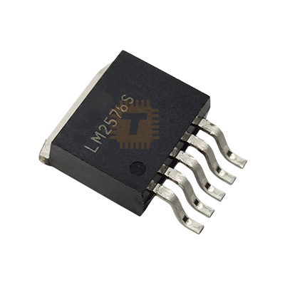
Original LM2576S-ADJ Adjustable Switch Mode Voltage Regulator TO-263-5 (IC0361) Products
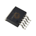
| Name | Original LM2576S-ADJ Adjustable Switch Mode Voltage Regulator TO-263-5 |
| Code | IC0361 |
| Price | Rs.400.00 |
| In Stock | Yes |
| Package | SOT23-5 |
Product Details
The Original LM2576S-ADJ Step-Down (Buck) Switch Mode Voltage Regulator is a monolithic integrated circuit manufactured by Texas Instruments / ON Semiconductor, designed for high-efficiency DC-DC step-down power conversion. Encapsulated in a surface-mount TO-263-5 (D2PAK) power package with an exposed thermal tab, it is capable of driving up to a 3.0A continuous load with excellent line and load regulation. Operating at a fixed internal switching frequency of 52 kHz, the adjustable version enables precise output voltage tuning from 1.23V up to 37V using an external two-resistor divider network. It incorporates internal frequency compensation, cycle-by-cycle current limiting, under-voltage lockout, and thermal shutdown protection. The LM2576S-ADJ serves as an energy-efficient replacement for classic 3-terminal linear regulators (like LM317 or 78xx series), eliminating large heat sinks in industrial power supplies, distributed power systems, battery chargers, and robotics motor rails.
Specifications
- Part Number / Model: LM2576S-ADJ / LM2576SX-ADJ (Adjustable Output Version)
- Manufacturer: Texas Instruments / ON Semiconductor
- Regulator Topology: Step-Down (Buck) Switching DC-DC Converter
- Package Type: TO-263-5 / D2PAK / DDPAK (5-Lead Surface-Mount Power Package with Exposed Tab)
- Adjustable Output Voltage Range (Vout): 1.23V to 37V DC (±4% max tolerance over line and load conditions)
- Internal Reference Voltage (Vref): Typ. 1.230V / Range 1.217V to 1.243V (at 25°C)
- Maximum Continuous Output Current (Iout): 3.0 A
- Input Voltage Range (Vin): 4.0V to 40V DC (Standard Voltage Version)
- Internal Oscillator / Switching Frequency (fosc): Typ. 52 kHz (±10% / 47 kHz to 58 kHz)
- Saturation Voltage (Vsat): Typ. 1.4V / Max. 1.8V (at Iout = 3A)
- Typical Conversion Efficiency: 75% to 88% (depending on Vin, Vout, and load current)
- Quiescent Current (Operating): Typ. 5.0 mA / Max. 10.0 mA (Feedback = 1.3V, Not Switching)
- Standby Quiescent Current: Typ. 50 µA / Max. 200 µA (when ON/OFF pin is pulled HIGH)
- Current Limit Threshold: Typ. 4.2 A / Range 3.5 A to 6.5 A (Cycle-by-cycle current limit)
- ON/OFF Logic Threshold Voltage: Low (Regulator ON): < 0> 2.0V
- Operating Junction Temperature (Tj): -40°C to +125°C
- Storage Temperature Range (Tstg): -65°C to +150°C
- Thermal Resistance, Junction-to-Case (Rth(j-c)): ~2°C/W
- Thermal Resistance, Junction-to-Ambient (Rth(j-a)): ~45°C/W to 50°C/W (mounted on standard PCB copper plane)
- Pinout Configuration (TO-263-5 - Leads Pointing Down, Left to Right):
- Pin 1: VIN (Input Supply Voltage, 4V to 40V)
- Pin 2: OUTPUT (Switching Node / Inductor Drive Output)
- Pin 3: GROUND & Thermal Tab (System Power Ground)
- Pin 4: FEEDBACK (Output Voltage Sense / Resistor Divider Input)
- Pin 5: ON/OFF (Active-Low Enable: Tie to GND for ON, Pull to VIN/Logic High for Shutdown)
- Exposed Center Tab: Internally connected to Pin 3 (GND)
Features
- High 3.0A Output Capability: Delivers up to 3.0A of continuous DC current with significantly less power dissipation compared to traditional linear power regulators.
- Adjustable Output Flexibility (1.23V to 37V): Simple external resistor divider sets the desired output voltage precisely for standard 3.3V, 5V, 9V, 12V, 18V, or 24V supply rails.
- TTL-Compatible ON/OFF Shutdown: Dedicated Pin 5 allows microcontrollers or supervisory circuits to place the regulator into an ultra-low 50µA standby sleep state.
- Requires Only 4 External Components: Operates with just an input capacitor, output inductor, catch Schottky diode, and output capacitor (plus two feedback resistors for adjustable mode).
- Robust Internal Protections: Includes cycle-by-cycle peak current limiting, second-stage frequency foldback under output short-circuit conditions, and thermal overload shutdown.
- High-Thermal Surface-Mount D2PAK Package: Wide bottom thermal tab solders directly to PCB ground copper pours for efficient heat conduction without requiring bulky heatsinks.
Common Applications
- Pre-Regulator for Linear Regulators: Efficient primary step-down stage from high-voltage DC (24V–36V) to reduce heat dissipation in downstream LDO stages.
- High-Efficiency Step-Down (Buck) Regulators: Core power supplies for industrial control boards, embedded motherboards, and CNC motion controllers.
- Robotics & High-Current Motor Rails: Step-down power conversion from 3S/4S/6S LiPo batteries to 5V or 6V for heavy-duty digital servos and sensor clusters.
- Battery Chargers: Constant voltage step-down source for Lead-Acid, LiFePO4, and multi-cell Lithium battery charging systems.
- Automotive & Solar Power Converters: Stepping down 12V/24V vehicle battery buses or solar panels to stabilized 5V/12V auxiliary power.
Usage Tips
- Feedback Resistor Divider Calculation: The output voltage is calculated using Vout = 1.23V × (1 + R2 / R1), where R1 is connected between Pin 4 (Feedback) and GND, and R2 is connected between Vout and Pin 4. A recommended standard value for R1 is **1.0kΩ to 5.0kΩ** (1% tolerance recommended).
- For 5.0V Output (with R1 = 1.0kΩ): R2 = 1.0kΩ × (5.0 / 1.23 - 1) ≈ 3.06kΩ (Standard 3.09kΩ 1%).
- For 12.0V Output (with R1 = 1.0kΩ): R2 = 1.0kΩ × (12.0 / 1.23 - 1) ≈ 8.75kΩ (Standard 8.66kΩ or 8.87kΩ 1%).
- Catch Diode Selection (Critical): Always use a **fast-recovery Schottky diode rated for at least 3A and 40V+ (e.g., 1N5822, SS34, or SK34)** connected from Pin 2 (Cathode) to GND (Anode). Standard 1N4007 or 1N5408 silicon rectifier diodes are too slow and will cause immediate regulator failure.
- Inductor Sizing: Use a shielded power inductor rated for at least 3.5A to 4.0A saturation current with an inductance value between **68µH and 150µH** (depending on Vin and Vout parameters from the LM2576 inductor selection guide).
- Low-ESR Output Capacitors: Use high-frequency, low-ESR electrolytic capacitors (typically 470µF to 1000µF, 35V/50V) or solid polymer capacitors on the output to minimize switching ripple and prevent loop instability.
- PCB Thermal & Grounding Layout: Keep the loop formed by Pin 1 (VIN), Pin 2 (OUTPUT), the Schottky diode, and the ground plane as short and wide as possible. Solder Pin 3 and the large exposed thermal tab to a wide ground copper pour with multiple thermal vias.
Sharing is caring, show love and share the product with your friends.
Featured

Add to Cart

Add to Cart