Original Microchip PIC16F15213 PDIP-8 (MC0004) Products
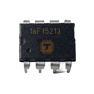
| Name | Original Microchip PIC16F15213 PDIP-8 |
| Code | MC0004 |
| Price | Rs.800.00 |
| In Stock | Yes |
| Package | SOIC-28 |
Product Details
The Original Microchip PIC16F15213 8-Bit Flash Microcontroller is an ultra-compact, cost-effective, high-performance 8-pin MCU manufactured by Microchip Technology. Encapsulated in a prototyping-friendly standard PDIP-8 (DIP-8) through-hole package, it is powered by an enhanced mid-range 8-bit core operating at speeds up to 32 MHz with a precision internal oscillator. Designed specifically for space-constrained and cost-sensitive applications, the PIC16F15213 incorporates a suite of Core Independent Peripherals (CIPs)—including a 10-bit Analog-to-Digital Converter with Computation (ADCC), Complementary Waveform Generator (CWG), Capture/Compare/PWM (CCP) modules, a 10-bit PWM, and an industry-standard serial EUSART/MSSP (I2C/SPI) communication module. With integrated Peripheral Pin Select (PPS) functionality, pin mappings can be flexibly reconfigured to simplify board layout. It is widely utilized in smart home appliances, sensor signal conditioning, low-power IoT nodes, power management modules, and DIY embedded prototypes.
Specifications
- Part Number / Model: PIC16F15213-I/P / PIC16F15213 (Industrial Temperature Grade)
- Manufacturer: Microchip Technology
- Core Architecture: Enhanced Mid-Range 8-Bit PIC Core (49 Instructions)
- Package Type: PDIP-8
- Operating Supply Voltage Range (VDD): 1.8V to 5.5V DC (Wide operating supply range)
- Maximum CPU Operating Frequency: Up to 32 MHz (via internal HFINTOSC or external clock)
- Internal Oscillator: Factory-calibrated High-Frequency Internal Oscillator (HFINTOSC) up to 32 MHz (±1% typical accuracy) and Low-Frequency LFINTOSC (31 kHz)
- Program Memory (Flash): 3.5 KB (2,048 Words Flash Program Memory, Self-Read/Write capability)
- Data SRAM: 256 Bytes
- Data EEPROM / HEF: 128 Bytes High-Endurance Flash (HEF) memory (100k endurance cycles)
- General Purpose I/O (GPIO): 6 User I/O Pins (5 Bi-directional I/O + 1 Input-Only Pin RA3/MCLR)
- Peripheral Pin Select (PPS): Digital peripheral crossbar routing matrix on Port A pins
- Analog-to-Digital Converter (ADC): 10-Bit ADC with Computation (ADCC) and up to 5 Analog Input Channels
- Internal Fixed Voltage Reference (FVR): 1.024V, 2.048V, and 4.096V programmable references
- PWM / Timers / CCP:
- 2x 10-bit PWM Modules
- 2x Capture/Compare/PWM (CCP) Modules
- 1x Complementary Waveform Generator (CWG) with dead-band control
- Timer0 (8/16-bit), Timer1 (16-bit with gate), Timer2 (8-bit hardware limit timer)
- Serial Communication Peripherals:
- 1x EUSART (Enhanced Universal Synchronous/Asynchronous Receiver/Transmitter with LIN/DMX support)
- 1x MSSP (Master Synchronous Serial Port supporting I2C Master/Slave and SPI Master/Slave)
- Power Management (eXtreme Low-Power - XLP): Ultra-low power modes with Sleep current down to < 20>
- Operating Ambient Temperature (TA): -40°C to +85°C (Industrial Grade) / up to +125°C (Extended Grade)
- Storage Temperature Range (Tstg): -65°C to +150°C
- Pinout Configuration (PDIP-8):
- Pin 1: VDD (Positive Power Supply Input, +1.8V to +5.5V)
- Pin 2: RA5 (GPIO / CLKIN / OSC1 / PWM / T1CKI via PPS)
- Pin 3: RA4 (GPIO / CLKOUT / OSC2 / T1G via PPS)
- Pin 4: RA3 / MCLR / VPP (Active-Low Master Clear Reset / Programming Voltage / Input Only)
- Pin 5: RA2 (GPIO / AN2 / INT / DAC1OUT / FVR / PPS Configurable)
- Pin 6: RA1 / ICSPCLK (GPIO / AN1 / In-Circuit Serial Programming Clock / PPS Configurable)
- Pin 7: RA0 / ICSPDAT (GPIO / AN0 / In-Circuit Serial Programming Data / PPS Configurable)
- Pin 8: VSS (Ground / 0V Reference)
Features
- Core Independent Peripherals (CIPs): Hardware-based modules (CWG, CCP, 10-bit PWM, ADCC) operate autonomously from the CPU core, executing tasks with zero CPU overhead and reducing overall power consumption.
- Peripheral Pin Select (PPS) in 8-Pin Footprint: Full digital pin mapping flexibility allows serial lines (UART TX/RX, SPI SCK/SDO/SDI, I2C SDA/SCL) and PWM signals to be routed to any of the available I/O pins, greatly simplifying PCB design.
- 10-Bit ADC with Computation (ADCC): Hardware-accelerated ADC automates functions such as signal averaging, oversampling, threshold comparison, and low-pass filtering directly in hardware.
- Complementary Waveform Generator (CWG): Generates non-overlapping complementary switching signals with programmable dead-band delays to safely control half-bridge power drivers.
- Dual Serial Engines (EUSART & MSSP): Full hardware UART alongside hardware I2C/SPI enables multi-device sensor reading and communication without software bit-banging.
- Breadboard & Prototyping Friendly: Standard 0.1-inch (2.54mm) pitch PDIP-8 package easily fits into solderless breadboards, standard 8-pin IC sockets, and DIY proto-boards.
Common Applications
- Smart Home Appliances & Consumer Devices: Auxiliary button scanning, LED indicators, thermostat monitoring, and motor supervisory sub-circuits.
- Sensor Interface & Conditioning Nodes: Sampling analog transducers via ADCC and relaying telemetry over I2C, SPI, or UART lines.
- Power Conversion & LED Lighting: Direct PWM and CWG generation for small DC-DC converters, LED dimmers, and motor speed controllers.
- Automotive & Industrial Auxiliaries: Small node LIN/UART protocol converters, safety interlocks, and hardware watchdog supervisory units.
- DIY Robotics & Prototyping: Ultra-compact microcontroller brain for sensor parsing, servo control, and breadboard electronics projects.
Usage Tips
- In-Circuit Serial Programming (ICSP): For flashing and debugging via Microchip PICkit (PICkit 3, 4, 5) or SNAP debuggers, connect:
- VPP/MCLR to Pin 4 (RA3)
- VDD (+3.3V or +5.0V) to Pin 1
- VSS (GND) to Pin 8
- ICSPDAT to Pin 7 (RA0)
- ICSPCLK to Pin 6 (RA1)
- Power Supply Decoupling: Place a **0.1µF (100nF) ceramic capacitor** directly across Pin 1 (VDD) and Pin 8 (VSS) with minimal trace length to suppress power rail transients and ensure stable ADC sampling.
- Peripheral Pin Select (PPS) Setup: Since the chip has only 5 bi-directional I/O pins, configure the PPS registers in code (e.g., using MCC / Microchip Code Configurator) to route your required peripherals (UART, I2C, SPI, PWM) to the chosen physical pins.
- MCLR Reset Pin Configuration: When Pin 4 (RA3/MCLR) is configured as the active-low reset pin, connect a **10kΩ pull-up resistor** from Pin 4 to VDD (with an optional 100nF filter capacitor to GND for high-noise industrial environments). If configured as a general-purpose input (MCLRE = OFF), it operates strictly as an input-only pin.
- ADC Fixed Voltage Reference (FVR): Enable the internal FVR (selectable between 1.024V, 2.048V, or 4.096V) as the positive reference ($V_{REF+}$) for the ADCC to achieve steady and repeatable analog conversions even if the main VDD supply fluctuates.
Sharing is caring, show love and share the product with your friends.
Featured

Add to Cart

Add to Cart


Add to Cart
Other Products
Add to Cart