
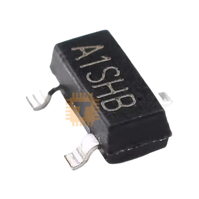
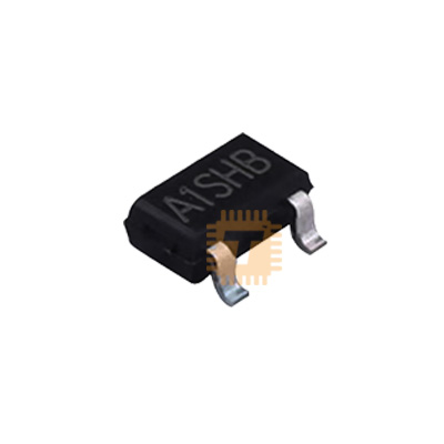
Original SI2301 A1SHB P-Channel MOSFET SOT-23 (DI0270) Products
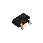
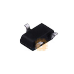
| Name | Original SI2301 A1SHB P-Channel MOSFET SOT-23 |
| Code | DI0270 |
| Price | Rs.10.00 |
| In Stock | Yes |
| Package | SMD |
Product Details
The SI2301 (marked as A1SHB) is a high-density, sub-logic level P-Channel enhancement mode field-effect transistor utilizing advanced trench MOSFET technology. Designed to deliver low on-state resistance (RDS(ON)), fast switching speeds, and low gate drive capability within an ultra-compact SOT-23 surface-mount package, it is ideally suited for high-side load switching, power distribution management, battery disconnect circuits, and reverse polarity protection in portable battery-powered electronics.
Specifications
- Brand / Manufacturer: Vishay Siliconix / Industry Standard
- Part Number / Marking: SI2301 / SI2301CDS / A1SHB
- Transistor Type: P-Channel MOSFET
- Drain-Source Breakdown Voltage (VDS): -20V
- Gate-Source Voltage (VGS): ±8V (Up to ±12V depending on manufacturer grade)
- Continuous Drain Current (ID): -2.8A (at VGS = -4.5V, TA = 25°C) / -2.3A (at VGS = -2.5V)
- Pulsed Drain Current (IDM): -10A
- Low On-Resistance (RDS(ON)): < 90m>GS = -4.5V (ID = -2.8A)
- Low On-Resistance (RDS(ON)): < 130m>GS = -2.5V (ID = -2.0A)
- Gate Threshold Voltage (VGS(th)): -0.45V to -1.0V (Typical -0.7V)
- Total Gate Charge (Qg): Approx. 4.5nC (at VGS = -4.5V)
- Maximum Power Dissipation (PD): 1.25W (at TA = 25°C)
- Operating Junction & Storage Temperature: -55°C to +150°C
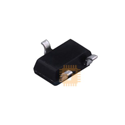
- Package / Case: SOT-23 (TO-236) Surface Mount (Pin 1: Gate, Pin 2: Source, Pin 3: Drain)
Features
- Advanced TrenchFET Technology: Delivers high cell density and low on-resistance to minimize power dissipation and heat generation during conduction.
- Sub-Logic Level Gate Drive: Operates efficiently with low gate voltages down to -2.5V, enabling direct high-side drive from 3.3V and 5V microcontrollers and low-voltage logic circuitry.
- Simplified High-Side Switching: As a P-Channel device, it enables direct load gating on the positive rail without requiring an external charge pump or bootstrap circuit.
- Compact SOT-23 Footprint: Provides high power handling and reliable thermal dissipation in a miniature surface-mount package, saving valuable PCB area.
- Fast Switching Speed: Low gate-to-drain charge ensures quick turn-on and turn-off transitions, minimizing switching losses in PWM power management circuits.
Common Applications
- High-Side Power Rail Switches: Gating sub-circuits, peripheral sensors, and wireless communication modules in portable electronics.
- Battery Disconnect & Charging Circuits: Regulating charge paths and battery isolation in lithium-ion and multi-cell battery packs.
- Reverse Polarity Protection: Low-forward-drop protection on DC input rails as an efficient alternative to traditional Schottky diodes.
- DC-DC Converters & Inverters: High-side switching stages in compact buck and boost power topologies.
- Small Actuator & Indicator Drivers: High-side switching for relays, indicator LEDs, solenoids, and buzzers.
Usage Tips
- High-Side Connection: Connect the Source (Pin 2) directly to the positive input voltage rail (VIN) and the Drain (Pin 3) to the load. Pull the Gate (Pin 1) to GND to turn the MOSFET ON, and pull it high to VIN to turn it OFF.
- Pull-Up Resistor Placement: Always install a 10kΩ to 100kΩ pull-up resistor between the Gate and Source pins to prevent floating gate states and unwanted turn-on during microcontroller startup.
- Gate Voltage Limit Compliance: Ensure that the Gate-to-Source differential voltage (VGS) remains strictly within the rated ±8V limit. If switching supply voltages above 5V, use a resistor divider or Zener diode clamp on the Gate.
- Flyback Suppression: When driving inductive loads such as relays or DC motors, place a fast-recovery freewheeling diode (e.g., Schottky diode) across the load to protect the MOSFET against inductive kickback spikes exceeding VDS.
Sharing is caring, show love and share the product with your friends.
Featured

Add to Cart

Add to Cart

Other Products


Add to Cart

