Original TL494CN Switching PWM Controller DIP-16 (IC0352) Products
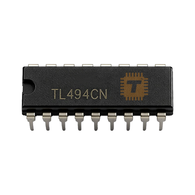
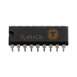
| Name | Original TL494CN Switching PWM Controller DIP-16 |
| Code | IC0352 |
| Price | Rs.100.00 |
| In Stock | Yes |
| Package | DIP-16 |
Product Details
The Original TL494CN Switching PWM Controller is an industry-standard fixed-frequency pulse-width modulation (PWM) control integrated circuit manufactured by Texas Instruments / ON Semiconductor. Encapsulated in a standard DIP-16 through-hole package, it incorporates all the primary functions required in the construction of switch-mode power supply (SMPS) control circuits on a single monolithic chip. Operating across a wide supply voltage range of 7V to 40V DC, the TL494CN features an on-chip precision 5.0V linear regulator (±5% initial accuracy), a linear sawtooth oscillator capable of frequencies up to 300 kHz, dual uncommitted error amplifiers, an adjustable dead-time control (DTC) comparator, an internal pulse-steering flip-flop, and dual uncommitted output transistors capable of sourcing or sinking up to 200mA each. It is widely utilized in PC ATX power supplies, push-pull DC-DC converters, half-bridge/full-bridge inverters, battery chargers, and high-power motor drivers.
Specifications
- Part Number / Model: TL494CN (Commercial Temperature Range)
- Device Function: Fixed-Frequency Pulse-Width Modulation (PWM) Control Circuit
- Package Type: DIP-16
- Supply Voltage Range (Vcc / Pin 12): 7.0V to 40V DC (Absolute Max: 41V)
- Collector Output Voltage (Vc1, Vc2 / Pins 8 & 11): Up to 40V DC (Absolute Max: 41V)
- Output Transistor Current (Ic1, Ic2): Continuous: 200mA (Max per transistor) / Peak: 500mA
- Reference Voltage Output (Vref / Pin 14): Typ. 5.0V / Range 4.75V to 5.25V (±5% initial accuracy)
- Reference Output Current: Up to 10mA DC
- Oscillator Frequency Range: 1.0 kHz to 300 kHz (Programmed via external RT and CT)
- Output Control Mode (Pin 13 - Output Ctrl): Ground (0V) for Single-Ended / Parallel mode (0% to 90% Max Duty Cycle); Tied to Vref (+5V) for Push-Pull / Interleaved mode (0% to 45% Max Duty Cycle per output)
- Dead-Time Control Input (DTC / Pin 4): 0V to 3.3V (0V input sets minimum ~3% to 4% internal dead time; 3.3V sets 100?ad time / 0% duty cycle)
- Error Amplifier Common-Mode Input Voltage: -0.3V to (Vcc - 2.0V)
- Error Amplifier Open-Loop Voltage Gain: Typ. 95 dB (at Vout = 0.5V to 3.5V)
- Error Amplifier Unity Gain Bandwidth: Typ. 800 kHz
- Output Saturation Voltage (Common-Emitter Mode): Typ. 1.1V / Max. 1.3V (at Ic = 200mA)
- Output Saturation Voltage (Emitter-Follower Mode): Typ. 1.5V / Max. 2.5V (at Ie = 200mA)
- Total Quiescent Current: Typ. 9.0mA / Max. 15mA (at Vcc = 15V)
- Total Power Dissipation (Pd): 1000mW (at Ta = 25°C)
- Operating Ambient Temperature (Ta): 0°C to +70°C
- Storage Temperature Range (Tstg): -65°C to +150°C
- Thermal Resistance, Junction to Ambient (Rth(j-a)): 70°C/W to 80°C/W
- Pinout Configuration:
- Pin 1: Non-Inverting Input, Error Amp 1 (1IN+)
- Pin 2: Inverting Input, Error Amp 1 (1IN-)
- Pin 3: Feedback / PWM Comparator Input (FEEDBACK / COMP)
- Pin 4: Dead-Time Control (DTC)
- Pin 5: Timing Capacitor (CT)
- Pin 6: Timing Resistor (RT)
- Pin 7: Ground (GND)
- Pin 8: Collector Output 1 (C1)
- Pin 9: Emitter Output 1 (E1)
- Pin 10: Emitter Output 2 (E2)
- Pin 11: Collector Output 2 (C2)
- Pin 12: Operating Supply Voltage (VCC)
- Pin 13: Output Control Mode (OUTPUT CTRL)
- Pin 14: Reference Voltage Output (+5.0V VREF)
- Pin 15: Inverting Input, Error Amp 2 (2IN-)
- Pin 16: Non-Inverting Input, Error Amp 2 (2IN+)
Features
- Dual Uncommitted Error Amplifiers: Two independent wide-bandwidth error amplifiers allow simultaneous, independent regulation of output voltage and cycle-by-cycle current limiting.
- Flexible Output Configurations: Uncommitted collector and emitter terminals on both output transistors allow configuration as push-pull, half-bridge, single-ended buck/boost, or emitter-follower driver topologies.
- Built-in Pulse-Steering Flip-Flop: Prevents multiple pulsing of either output transistor during high-frequency switching and guarantees alternating half-cycle drive in push-pull mode.
- Adjustable Dead-Time Control (DTC): Pin 4 provides linear adjustment of dead time from minimum 3% up to 100%, preventing shoot-through current in totem-pole and bridge inverter stages.
- Selectable Push-Pull or Parallel Drive: Setting Pin 13 (Output Control) HIGH sets alternating push-pull drive (up to 45% duty cycle each); setting Pin 13 LOW enables parallel single-ended operation (up to 90% duty cycle).
- Precision 5V Reference Generator: On-chip linear reference provides a stable, temperature-compensated 5.0V source to bias voltage divider networks and error amp inputs.
Common Applications
- ATX Desktop & Server Power Supplies: Main PWM controller managing the primary half-bridge power transformer and feedback regulation stages.
- Push-Pull DC-DC Boost Converters: 12V/24V to 220V/310V step-up power inverter boards for solar and off-grid power systems.
- Lead-Acid & Lithium Battery Chargers: Constant-Voltage / Constant-Current (CC/CV) multi-stage charging controllers using dual onboard error amplifiers.
- High-Power Pure & Modified Sine Wave Inverters: High-frequency front-end DC bus voltage boost controllers.
- Industrial Switch-Mode Power Supplies: Forward, flyback, and full-bridge industrial power converter racks.
Usage Tips
- Oscillator Calculation Formula: Set the switching frequency using: f_osc = 1 / (RT × CT) for single-ended mode, or f_out = 1 / (2 × RT × CT) per output in push-pull mode. Recommended values are RT = 1kΩ to 500kΩ and CT = 470pF to 10µF (typical RT = 10kΩ to 100kΩ, CT = 1nF to 10nF).
- Configuring Output Control (Pin 13): For push-pull, half-bridge, or full-bridge circuits, wire Pin 13 directly to Pin 14 (+5V Vref) to enable alternating flip-flop drive. For single-ended buck, boost, or parallel drive, connect Pin 13 directly to Pin 7 (GND).
- Soft-Start Circuit Implementation: To implement power-on soft-start, connect an electrolytic capacitor (e.g., 10µF) between Pin 14 (Vref) and Pin 4 (DTC), and place a 10kΩ resistor from Pin 4 (DTC) to Pin 7 (GND). Upon power-up, DTC starts at 5V (0% duty cycle) and smoothly decays to 0V (full duty cycle).
- Terminating Unused Error Amplifiers: If using only Error Amp 1 for voltage feedback, disable Error Amp 2 cleanly to avoid oscillation by tying Pin 16 (2IN+) to Pin 7 (GND) and Pin 15 (2IN-) to Pin 14 (Vref).
- Reference Noise Bypass: Place a 100nF low-ESR ceramic capacitor directly across Pin 14 (Vref) and Pin 7 (GND) to suppress high-frequency switching noise on the internal voltage reference rail.
Sharing is caring, show love and share the product with your friends.
Featured

Add to Cart


Add to Cart

Add to Cart