Original TL494CN Switching PWM Controller SOP-16 (IC0353) Products
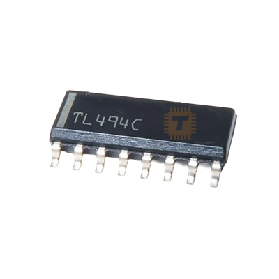
| Name | Original TL494CN Switching PWM Controller SOP-16 |
| Code | IC0353 |
| Price | Rs.70.00 |
| In Stock | Yes |
| Package | SOP-16 |
Product Details
The Original TL494CD / TL494CDR Switching PWM Controller (commonly referenced in SOP-16 package format) is an industry-standard fixed-frequency pulse-width modulation (PWM) control integrated circuit manufactured by Texas Instruments / ON Semiconductor. Encapsulated in a compact SOP-16 (SOIC-16 / SO-16) surface-mount package, it incorporates all the primary functions required in the construction of switch-mode power supply (SMPS) control circuits on a single monolithic chip. Operating across a wide supply voltage range of 7V to 40V DC, the TL494 features an on-chip precision 5.0V linear reference regulator (±5% initial accuracy), a linear sawtooth oscillator capable of switching frequencies up to 300 kHz, dual uncommitted error amplifiers, an adjustable dead-time control (DTC) comparator, an internal pulse-steering flip-flop, and dual uncommitted output transistors capable of sourcing or sinking up to 200mA each. It is widely utilized in compact PC ATX power supplies, push-pull DC-DC converters, half-bridge/full-bridge inverters, battery chargers, and high-density power electronics boards.
Specifications
- Part Number / Model: TL494CD / TL494CDR / TL494CN (SOP-16 Surface Mount Variant)
- Device Function: Fixed-Frequency Pulse-Width Modulation (PWM) Control Circuit
- Package Type: SOP-16
- Supply Voltage Range (Vcc / Pin 12): 7.0V to 40V DC (Absolute Max: 41V)
- Collector Output Voltage (Vc1, Vc2 / Pins 8 & 11): Up to 40V DC (Absolute Max: 41V)
- Output Transistor Current (Ic1, Ic2): Continuous: 200mA (Max per transistor) / Peak: 500mA
- Reference Voltage Output (Vref / Pin 14): Typ. 5.0V / Range 4.75V to 5.25V (±5% initial accuracy)
- Reference Output Current: Up to 10mA DC
- Oscillator Frequency Range: 1.0 kHz to 300 kHz (Programmed via external RT and CT)
- Output Control Mode (Pin 13 - Output Ctrl): Ground (0V) for Single-Ended / Parallel mode (0% to 90% Max Duty Cycle); Tied to Vref (+5V) for Push-Pull / Interleaved mode (0% to 45% Max Duty Cycle per output)
- Dead-Time Control Input (DTC / Pin 4): 0V to 3.3V (0V sets minimum ~3% to 4% internal dead time; 3.3V sets 100?ad time / 0% duty cycle)
- Error Amplifier Common-Mode Input Voltage: -0.3V to (Vcc - 2.0V)
- Error Amplifier Open-Loop Voltage Gain: Typ. 95 dB (at Vout = 0.5V to 3.5V)
- Error Amplifier Unity Gain Bandwidth: Typ. 800 kHz
- Output Saturation Voltage (Common-Emitter Mode): Typ. 1.1V / Max. 1.3V (at Ic = 200mA)
- Output Saturation Voltage (Emitter-Follower Mode): Typ. 1.5V / Max. 2.5V (at Ie = 200mA)
- Total Quiescent Current: Typ. 9.0mA / Max. 15mA (at Vcc = 15V)
- Total Power Dissipation (Pd): 700mW to 900mW (at Ta = 25°C in standard SOP-16)
- Operating Ambient Temperature (Ta): 0°C to +70°C
- Storage Temperature Range (Tstg): -65°C to +150°C
- Thermal Resistance, Junction to Ambient (Rth(j-a)): ~100°C/W to 120°C/W
- Pinout Configuration:
- Pin 1: Non-Inverting Input, Error Amp 1 (1IN+)
- Pin 2: Inverting Input, Error Amp 1 (1IN-)
- Pin 3: Feedback / PWM Comparator Input (FEEDBACK / COMP)
- Pin 4: Dead-Time Control (DTC)
- Pin 5: Timing Capacitor (CT)
- Pin 6: Timing Resistor (RT)
- Pin 7: Ground (GND)
- Pin 8: Collector Output 1 (C1)
- Pin 9: Emitter Output 1 (E1)
- Pin 10: Emitter Output 2 (E2)
- Pin 11: Collector Output 2 (C2)
- Pin 12: Operating Supply Voltage (VCC)
- Pin 13: Output Control Mode (OUTPUT CTRL)
- Pin 14: Reference Voltage Output (+5.0V VREF)
- Pin 15: Inverting Input, Error Amp 2 (2IN-)
- Pin 16: Non-Inverting Input, Error Amp 2 (2IN+)
Features
- Compact SOP-16 SMD Footprint: Space-saving surface-mount package ideal for modern high-density power supply PCBs, modular inverter boards, and compact DC-DC converters.
- Dual Uncommitted Error Amplifiers: Two independent wide-bandwidth operational error amplifiers enable simultaneous, independent output voltage regulation and current-limit feedback.
- Flexible Output Configurations: Uncommitted collector and emitter terminals on both internal output transistors support push-pull, half-bridge, buck, boost, or totem-pole gate driver topologies.
- Built-in Pulse-Steering Flip-Flop: Prevents multiple pulsing of either output transistor during high-frequency switching and guarantees alternating half-cycle drive in push-pull mode.
- Adjustable Dead-Time Control (DTC): Pin 4 provides precise dead-time adjustment from minimum 3% up to 100%, protecting external power switches against destructive shoot-through currents.
- Precision 5V Internal Reference: Integrated on-chip linear regulator provides a temperature-compensated 5.0V source to bias voltage divider networks and error amp inputs.
Common Applications
- Surface-Mount SMPS & DC-DC Converters: High-density step-up/step-down power supplies and industrial telecom modules.
- Push-Pull Solar Inverter Boards: High-frequency DC-DC front-end booster stages in 12V/24V to 220V/310V inverters.
- Compact Battery Charging Systems: Multi-stage CC/CV controllers for Lithium-ion, LiFePO4, and Lead-Acid battery banks.
- High-Power LED Driver Stages: Multi-channel constant-current PWM switching regulators.
- Industrial Motor Speed Controllers: H-bridge PWM motor drivers and automated power actuators.
Usage Tips
- Package Suffix Clarification: Standard manufacturer nomenclature uses TL494CD / TL494CDR for the SOP-16 / SOIC-16 package (where "N" traditionally denotes DIP-16). Ensure pad footprints in your PCB CAD match standard 150mil / 208mil SO-16 pitch spacing.
- Oscillator Design Formula: Configure switching frequency using: f_osc = 1 / (RT × CT) for single-ended mode, or f_out = 1 / (2 × RT × CT) per output channel in push-pull mode (Recommended: RT = 10kΩ to 100kΩ, CT = 1nF to 10nF).
- Configuring Output Mode (Pin 13): Connect Pin 13 to Pin 14 (+5V Vref) for push-pull / alternating half-bridge drive (up to 45% duty cycle each). Connect Pin 13 directly to Pin 7 (GND) for parallel / single-ended drive (up to 90% duty cycle).
- Soft-Start Setup: Connect a 10µF capacitor between Pin 14 (Vref) and Pin 4 (DTC), and a 10kΩ pull-down resistor from Pin 4 (DTC) to Pin 7 (GND) to achieve smooth, surge-free power-on ramp-up.
- SMD PCB Decoupling & Ground Plane: Mount a 100nF low-ESR ceramic decoupling capacitor right next to Pin 12 (VCC) and Pin 14 (Vref) referenced to a solid ground plane to prevent high-frequency switching noise from causing jitter in the internal sawtooth oscillator.
Sharing is caring, show love and share the product with your friends.
Featured


Add to Cart

Add to Cart