Original CS150N03 30V 150A N-Channel MOSFET TO-220 (DI0303) Products
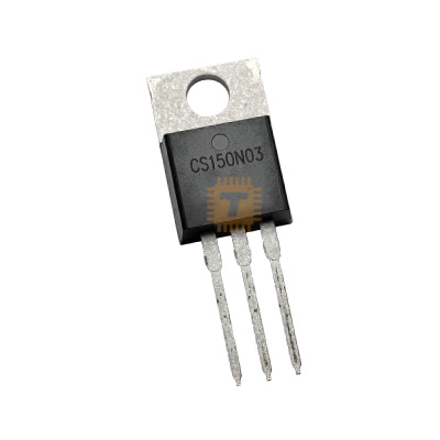
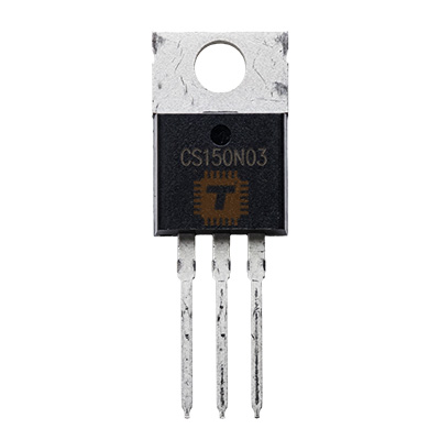
| Name | Original CS150N03 30V 150A N-Channel MOSFET TO-220 |
| Code | DI0303 |
| Price | Rs.270.00 |
| In Stock | Yes |
| Package | TO-220 |
Product Details
The Original CS150N03 30V 150A N-Channel Power MOSFET is a high-current, low-resistance trench power transistor housed in a standard through-hole TO-220 package. Utilizing advanced high-density trench gate technology, the CS150N03 delivers an ultra-low on-state resistance (Rds(on)) down to 2.4mΩ and high continuous current handling capability up to 150A. It is engineered for high-efficiency synchronous rectification, high-current DC motor drives, electronic speed controllers (ESC), battery protection circuits, and high-current power distribution systems.
Specifications
- Part Number / Model: CS150N03 / CS150N03A (High-Current Trench MOSFET Series)
- Transistor Type: N-Channel Enhancement Mode Power MOSFET
- Package Type: TO-220
- Drain-Source Breakdown Voltage (Vds): 30V
- Gate-Source Voltage (Vgs): ±20V
- Continuous Drain Current (Id):
- 150A (at Tc = 25°C, Package Silicon Limit)
- 105A to 110A (at Tc = 100°C)
- Pulsed Drain Current (Idm): 450A to 600A Peak
- Static Drain-Source On-Resistance (Rds(on)):
- Typ. 2.4mΩ / Max. 3.0mΩ (at Vgs = 10V, Id = 40A)
- Typ. 3.5mΩ / Max. 4.5mΩ (at Vgs = 4.5V, Id = 30A)
- Gate Threshold Voltage (Vgs(th)): 1.2V to 2.5V (Logic-Level Gate Drive Compatible)
- Total Gate Charge (Qg): Typ. 65nC to 80nC (at Vds = 15V, Id = 40A, Vgs = 10V)
- Input Capacitance (Ciss): Typ. 3800pF to 4500pF (at Vds = 15V, f = 1MHz)
- Single Pulse Avalanche Energy (Eas): ~450mJ to 600mJ
- Total Power Dissipation (Pd): 130W to 150W (at Tc = 25°C)
- Operating Junction & Storage Temperature: -55°C to +175°C
- Pinout Configuration: Pin 1: Gate (G), Pin 2: Drain (D), Pin 3: Source (S), Tab: Drain (D)
Features
- Ultra-Low On-State Resistance: Rds(on) down to 2.4mΩ drastically minimizes conduction losses (I²R) and reduces heat buildup during heavy continuous current delivery.
- High-Density Trench Technology: Provides high cell density, excellent avalanche ruggedness, and high peak pulsed current tolerance up to 450A+.
- Logic-Level Drive Capability: Operates efficiently with standard 4.5V to 10V gate drive signals, allowing direct driving from microcontrollers or dedicated gate drivers.
- High Thermal Dissipation TO-220 Tab: Solid metal backing tab allows direct bolting to heatsinks or heavy copper PCB planes for high power handling.
- Fast Switching Speed: Optimized gate charge enables high-frequency PWM operation in synchronous buck converters and motor controllers with low switching losses.
Common Applications
- High-Current DC Motor Drivers: H-bridge switching and PWM speed control for brushed DC motors, robotics, and RC model electronic speed controllers (ESCs).
- Synchronous Rectification: High-efficiency secondary-side rectification in low-voltage, high-current switch-mode power supplies (12V / 5V SMPS).
- Battery Management Systems (BMS): High-side/low-side discharge switches and short-circuit protection for Li-ion, LiFePO4, and lead-acid battery packs.
- Automotive & 12V/24V Power Distribution: Solid-state relay replacements, power disconnect switches, and high-amperage lighting/heater controls.
- High-Power DC-DC Buck Converters: Low-side and high-side power switching in multi-phase buck VRMs (Voltage Regulator Modules).
Usage Tips
- Heatsinking & Current Limits: When driving currents exceeding 30A continuously, mount the TO-220 tab firmly to a suitable aluminum heatsink with thermal compound; the physical package leads should be reinforced with solder/copper busbars on the PCB.
- Gate Driver Selection: Due to the high input capacitance (~4000pF), use a dedicated high-current gate driver (such as TC4420 or IR2104) to ensure fast gate charging and prevent prolonged transition periods.
- Gate Damping Resistor: Place a 4.7Ω to 10Ω series gate resistor close to Pin 1 (Gate) along with a 10kΩ pull-down resistor to prevent ringing and maintain a default OFF state.
- Flyback Clamping: When switching inductive motor loads or solenoids, include appropriate freewheeling Schottky diodes or RC snubber circuits across the load to protect the MOSFET from high-voltage inductive kickback.
Sharing is caring, show love and share the product with your friends.
Featured

Add to Cart

Add to Cart

Add to Cart

Add to Cart