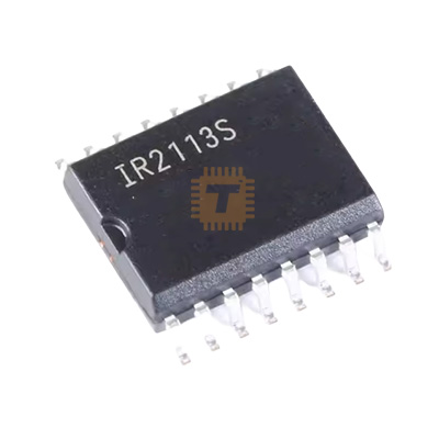
Original IR2113S Bridge Driver SOP-16 (IC0380) Products
| Name | Original IR2113S Bridge Driver SOP-16 |
| Code | IC0380 |
| Price | Rs.400.00 |
| In Stock | Yes |
| Package | SOIC-8 |
Product Details
The Original IR2113S High and Low Side Half-Bridge Driver IC is a high-voltage, high-speed power MOSFET and IGBT gate driver manufactured by Infineon Technologies / International Rectifier. Encapsulated in a standard SOP-16 (SOIC-16 Wide Body) surface-mount package, it features independent high-side and low-side referenced output channels. Utilizing proprietary high-voltage level-shifting and latch-immune CMOS technologies, the high-side floating channel operates up to 600V DC with an offset voltage capability of -5V to +600V. It delivers peak gate source/sink drive currents of up to 2.0A with fast, matched propagation delays (typ. 120ns / 94ns) and includes dedicated logic shutdown control and separate logic supply ground pins (VSS/COM) for superior noise immunity. The IR2113S is widely utilized in high-power switch-mode power supplies (SMPS), motor drives, H-bridge DC/AC inverters, induction heaters, Class-D audio amplifiers, and solar inverters.
Specifications
- Part Number / Model: IR2113S / IR2113STRPBF (International Rectifier / Infineon)
- Device Function: High-Voltage, High-Speed Dual-Channel (High-Side & Low-Side) Gate Driver
- Package Type: SOP-16
- High-Side Floating Offset Voltage (VB / VS): Up to 600V DC (Absolute Maximum: 625V)
- Gate Drive Supply Voltage (VCC): 10.0V to 20.0V DC (Absolute Maximum: 25.0V)
- Logic Supply Voltage (VDD): 3.3V to 20.0V DC (Independent 3.3V, 5V, or 15V logic compatibility)
- Peak Source / Sink Drive Current: Typ. +2.0 A / -2.0 A (at VBIAS = 15V)
- Turn-On Rise Time (ton / tr): Typ. 120 ns / 25 ns (at CL = 1000 pF)
- Turn-Off Fall Time (toff / tf): Typ. 94 ns / 17 ns (at CL = 1000 pF)
- Delay Matching (High-Side to Low-Side): Max. 10 ns (Tight timing matching for minimal dead-time requirement)
- Logic Input Compatibility: Standard 3.3V, 5V, and 15V CMOS / LSTTL with Schmitt-trigger inputs and pull-downs
- Shutdown Control (SD): Dedicated Active-High Shutdown Input (Forces both HO and LO outputs LOW)
- Under-Voltage Lockout (UVLO): Independent UVLO protection for both VCC and VBS channels
- Operating Junction Temperature (Tj): -40°C to +150°C
- Storage Temperature Range (Tstg): -55°C to +150°C
- Pinout Configuration (SOP-16 - Wide Body):
- Pin 1: LO (Low-Side Gate Drive Output)
- Pin 2: COM (Low-Side Power Ground Return)
- Pin 3: VCC (Low-Side Gate Drive Supply Voltage, 10V to 20V)
- Pin 4: NC (No Internal Connection)
- Pin 5: NC (No Internal Connection)
- Pin 6: VS (High-Side Floating Ground / Half-Bridge Switch Node)
- Pin 7: VB (High-Side Floating Bootstrap Power Supply)
- Pin 8: HO (High-Side Gate Drive Output)
- Pin 9: VDD (Logic Supply Voltage, 3.3V / 5V / 15V)
- Pin 10: HIN (Logic Input for High-Side Gate Driver - In-Phase)
- Pin 11: SD (Logic Input for Shutdown - Active High)
- Pin 12: LIN (Logic Input for Low-Side Gate Driver - In-Phase)
- Pin 13: VSS (Logic Ground Reference)
- Pin 14: NC (No Internal Connection)
- Pin 15: NC (No Internal Connection)
- Pin 16: NC (No Internal Connection)
Features
- 600V Floating High-Side Channel: Fully operational up to 600V DC, enabling direct high-side drive in universal AC off-line supplies and high-voltage DC bus converters.
- 2.0A Peak Gate Current Capability: Directly charges and discharges large capacitive gates on heavy power MOSFETs and IGBTs without requiring secondary booster transistors.
- Independent Logic Supply (VDD & VSS): Separate logic ground and supply pins allow seamless direct interfacing with 3.3V/5V microcontrollers (ESP32, STM32, Arduino, DSPs) isolated from high-current power ground noise.
- Tightly Matched Propagation Delays: 10ns max propagation delay matching allows high switching frequencies (up to several hundred kHz) while optimizing inverter dead-time.
- Active-High Hardware Shutdown (SD): Instantly disables both high-side and low-side outputs during hardware over-current or emergency stop events.
- Independent UVLO Circuitry: Ensures both the low-side and high-side driver stages maintain adequate gate drive voltage before switching to prevent MOSFET linear-mode burnout.
Common Applications
- H-Bridge & Half-Bridge Inverters: DC-to-AC pure sine wave inverters, solar grid-tie converters, and uninterrupted power supplies (UPS).
- High-Power Motor Drives: 3-Phase BLDC motor controllers, industrial AC induction motor inverters, and high-voltage brushed DC drivers.
- Switch-Mode Power Supplies (SMPS): Half-bridge and full-bridge LLC resonant converters and active-clamp forward stages.
- Induction Heating & Solid-State Tesla Coils: High-frequency resonant switching stages driving power IGBT / MOSFET pairs.
- Class-D Audio Amplifiers: High-power digital audio amplifier output switching stages.
Usage Tips
- Bootstrap Diode Selection: Use an ultra-fast recovery high-voltage diode (e.g., **UF4007, US1M, or ES1J** with trr < 50ns> 600V) connected from VCC (Anode) to VB (Cathode). Never use standard 1N4007 rectifier diodes as they are too slow for high-frequency bootstrap charging.
- Bootstrap Capacitor Sizing: Place a **0.1µF to 1µF low-ESR ceramic capacitor in parallel with a 10µF tantalum/electrolytic capacitor** directly across Pin 7 (VB) and Pin 6 (VS) to sustain high-side gate charge during conduction.
- Separate Logic & Power Grounds: Connect Pin 13 (VSS) to the microcontroller's logic ground and Pin 2 (COM) to the power MOSFET source ground. Tie VSS and COM together at a single star ground point near the driver to prevent power switching transients from corrupting logic inputs.
- Gate Resistor Damping: Place a small series damping resistor (typically **4.7Ω to 22Ω**) in series with both HO and LO pins to prevent parasitic gate-source ringing, with an optional reverse diode (1N4148) across the resistor for accelerated turn-off.
- Dead-Time Implementation: Unlike drivers with built-in interlocks, the IR2113S allows independent control of high and low side inputs. Ensure your microcontroller firmware implements adequate hardware/software **dead-time (typically 200ns to 1µs)** between complementary PWM channels to avoid shoot-through current across the half-bridge.
Sharing is caring, show love and share the product with your friends.