Original J112 N-Channel JFET Transistor TO-92 (DI0296) Products
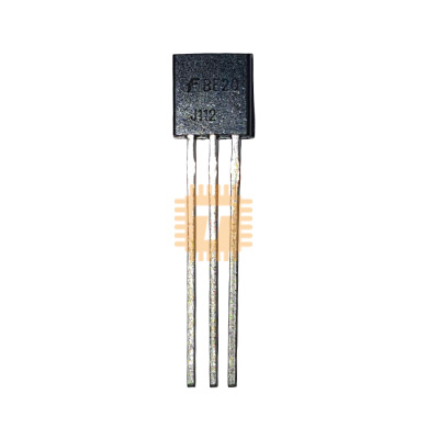
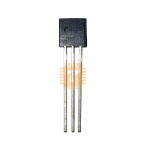
| Name | Original J112 N-Channel JFET Transistor TO-92 |
| Code | DI0296 |
| Price | Rs.70.00 |
| In Stock | Yes |
| Package | THT |
Product Details
The J112 is an industry-standard, high-speed N-Channel Junction Field-Effect Transistor (JFET) encapsulated in a compact TO-92 plastic through-hole package. Specifically engineered for low-resistance analog switching, chopper circuits, commutators, and audio muting applications, the J112 offers a low on-state resistance (RDS(on) < 50>
Specifications
- Brand / Manufacturer: ON Semiconductor / Fairchild / InterFET / Industry Standard
- Part Number: J112
- Transistor Type: N-Channel Symmetrical Depletion-Mode JFET
- Drain-Source Voltage (VDS): 35V
- Drain-Gate Voltage (VDG): 35V
- Gate-Source Reverse Breakdown Voltage (VGSR): -35V
- Gate Current (IG): 50mA
- Zero-Gate-Voltage Drain Current (IDSS): Minimum 5.0mA (Typically 5.0mA to 30mA @ VDS = 15V, VGS = 0V)
- Gate-Source Cutoff Voltage (VGS(off)): -1.0V to -5.0V (at VDS = 15V, ID = 1.0µA)
- Static Drain-Source On-Resistance (RDS(on)): < 50>GS = 0V, ID = 1.0mA)
- Common-Source Input Capacitance (Ciss): Max 28pF (at VDS = 0V, VGS = -10V, f = 1.0MHz)
- Common-Source Reverse Transfer Capacitance (Crss): Max 5.0pF (at VDS = 0V, VGS = -10V, f = 1.0MHz)
- Turn-On Time (ton): Typically < 4>
- Turn-Off Time (toff): Typically < 25ns>
- Total Device Dissipation (PD): 350mW to 625mW (at TA = 25°C)
- Operating Junction & Storage Temperature Range: -55°C to +150°C
- Package / Case: TO-92 (3-Pin Through-Hole: Pin 1: Drain, Pin 2: Source, Pin 3: Gate)
Features
- Low On-State Resistance (RDS(on) ≤ 50Ω): Ensures minimal insertion loss and low signal distortion across analog signal paths.
- Moderate Pinch-Off Voltage (-1.0V to -5.0V): Easier to turn fully OFF using standard low-to-medium negative logic supply rails compared to the J111.
- Ultra-Fast Switching Transitions: Nanosecond switching speeds provide crisp, low-latency analog gating without large propagation delays.
- Symmetrical Depletion-Mode Channel: Drain and Source terminals are fully interchangeable for bidirectional AC/DC analog signal handling.
- High Breakdown Margin (35V): Easily handles standard ±12V and ±15V op-amp signal swings without unwanted junction clipping.
Common Applications
- Analog Signal Switches & Routing: Precision low-loss signal switching in audio mixing consoles, synthesizers, and test gear.
- Audio Muting & Anti-Click Circuits: Silent, click-free muting for power amplifiers, DAC outputs, and preamps during power transitions.
- Sample-and-Hold / Chopper Amplifiers: High-speed charging/holding switches in data acquisition front-ends.
- Constant Current Sources / Limiters: Simple two-terminal constant current regulation when the Gate is shorted to the Source.
- Voltage-Controlled Attenuators: Smooth variable resistance element (VCR) in automated gain control (AGC) circuits.
Usage Tips
- Pinout Identification: Looking at the flat marked front face with leads pointing down, the pinout is Pin 1: Drain (D), Pin 2: Source (S), and Pin 3: Gate (G).
- Switching Control: The J112 is normally ON at VGS = 0V. To ensure complete turn-off across the entire waveform, pull the Gate negative relative to the Source by at least -5V to -7V (exceeding the peak negative voltage of the switched analog signal).
- Gate Over-Voltage Protection: Always place a series 10kΩ resistor or a fast switching diode in series with the gate to prevent forward-biasing the Gate-Channel PN junction (VGS must not exceed +0.7V).
- Constant Current Diode Mode: Tie Gate (Pin 3) directly to Source (Pin 2) to create a two-terminal current regulator delivering a fixed IDSS current.
Sharing is caring, show love and share the product with your friends.
Featured

Add to Cart


Add to Cart