Original UCC27321 High Speed MOSFET Driver SOIC-8 (IC0364) Products
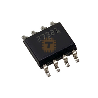
| Name | Original UCC27321 High Speed MOSFET Driver SOIC-8 |
| Code | IC0364 |
| Price | Rs.340.00 |
| In Stock | Yes |
| Package | SOIC-8 |
Product Details
The Original UCC27321 High-Speed Inverting MOSFET and IGBT Gate Driver IC is a precision, single-channel high-current gate driver manufactured by Texas Instruments. Encapsulated in an industry-standard SOIC-8 (SOP-8) package, it is engineered to deliver high peak currents of up to 9.0A into highly capacitive MOSFET and IGBT gates, making it ideal for high-frequency switch-mode power circuits. Utilizing a proprietary bipolar and CMOS compound output architecture (TrueDrive™), the driver delivers maximum drive current precisely during the Miller plateau region of the power switch transition. Featuring an ultra-fast propagation delay of only 20ns, matched rise/fall times under 20ns, and an integrated enable/disable function, the UCC27321 provides robust gate control in high-efficiency switch-mode power supplies (SMPS), synchronous rectification stages, DC-DC converters, motor drives, and solar inverters.
Specifications
- Part Number / Model: UCC27321D / UCC27321DR (Texas Instruments Marking: 27321)
- Manufacturer: Texas Instruments
- Driver Configuration: Single-Channel Inverting High-Speed Low-Side Gate Driver
- Output Architecture: TrueDrive™ Compound Bipolar and CMOS Output Stage
- Package Type: SOIC-8
- Supply Voltage Range (VDD): 4.0V to 15.0V DC (Absolute Maximum: 16.0V DC)
- Peak Source / Sink Drive Current: Typ. 9.0 A (at VDD = 14V)
- Output Rise Time (tr): Typ. 20 ns (with CL = 10,000 pF / 10 nF load)
- Output Fall Time (tf): Typ. 20 ns (with CL = 10,000 pF / 10 nF load)
- Propagation Delay Time (tD1, tD2): Typ. 20 ns to 25 ns (from input to output transition)
- Logic Input Compatibility: CMOS / TTL Compatible (Independent of VDD level; handles negative inputs down to -5V)
- Input Logic Thresholds:
- Logic High (VIH): Typ. 2.0V (Min. 2.2V)
- Logic Low (VIL): Typ. 1.1V (Max. 1.0V)
- Enable Control Function: Dedicated active-high Enable pin (ENBL) with internal pull-up to VDD
- Quiescent Supply Current (IDD): Typ. 0.3 mA to 1.0 mA (Static state)
- Operating Junction Temperature (Tj): -40°C to +125°C
- Storage Temperature Range (Tstg): -65°C to +150°C
- Pinout Configuration (SOIC-8):
- Pin 1: ENBL (Active-High Enable Input - Float or pull HIGH for normal operation, pull LOW to force OUT LOW)
- Pin 2: IN (Inverting Logic Control Input)
- Pin 3: NC (No Internal Connection)
- Pin 4: GND (Device Power and Signal Ground)
- Pin 5: GND (Device Power and Signal Ground - Internally tied to Pin 4)
- Pin 6: OUT (Inverting Gate Drive Output - TrueDrive Stage)
- Pin 7: OUT (Inverting Gate Drive Output - Internally paralleled with Pin 6)
- Pin 8: VDD (Power Supply Input, 4.0V to 15.0V)
Features
- 9.0A TrueDrive™ Compound Output: Combines paralleled Bipolar and MOSFET transistors to deliver massive peak current directly at the Miller plateau switching point, drastically cutting switching losses.
- Ultra-Fast 20ns Switching Performance: 20ns typical propagation delay and 20ns rise/fall times allow efficient operation at switching frequencies from hundreds of kilohertz up to megahertz levels.
- VDD-Independent Logic Inputs: Accommodates standard 3.3V and 5.0V logic levels directly from microcontrollers, DSPs, or PWM controllers without requiring level-shifter circuitry.
- Negative Input Voltage Immunity: Logic input pin can safely tolerate negative voltage transients down to -5V without device latch-up or damage.
- Dedicated Hardware Enable (ENBL): Provides independent active-high shutdown control for emergency braking, overcurrent latching, or system power sequencing.
- Paralleled Output and Ground Pins: Dual pin connections for OUT (Pins 6 & 7) and GND (Pins 4 & 5) reduce parasitic package inductance and improve thermal dissipation.
Common Applications
- High-Efficiency Switch-Mode Power Supplies (SMPS): Primary-side MOSFET driver in high-power Flyback, Forward, Half-Bridge, and Full-Bridge topologies.
- Synchronous Rectification Drivers: High-speed secondary-side gate drive for low-voltage, high-current buck and boost converters.
- DC-DC Brick Modules & Telecom Power: High-density power converter stages requiring rapid gate charging and discharging.
- Motor Drives & H-Bridge Inverters: Low-side gate control for brushless DC (BLDC) and stepper motor driver stages.
- Solar Inverters & Pulse Generators: Fast gate switching for power MOSFETs and IGBTs in renewable energy conversion systems.
Usage Tips
- Inverting Drive Logic Awareness: Remember that the UCC27321 is an **inverting** gate driver (Logic HIGH on Pin 2 drives Pin 6/7 OUT to GND; Logic LOW drives OUT to VDD). Ensure your MCU PWM polarity configuration accounts for this inverted logic.
- High-Frequency Bypass Capacitors (Critical): Peak currents of 9A produce severe VDD rail transients. Place a **1.0µF to 4.7µF low-ESR ceramic capacitor directly across Pin 8 (VDD) and Pins 4/5 (GND)** with minimal trace length, paralleled with a 10µF electrolytic or tantalum capacitor.
- Gate Resistor & Layout Minimization: Keep gate drive PCB traces between Pin 6/7 (OUT) and the external MOSFET gate as short and wide as possible. Use a small series gate resistor (e.g., 2.2Ω to 10Ω) to dampen high-frequency parasitic ringing caused by trace inductance.
- Paralleling Output & Ground Pins: Always tie Pin 6 and Pin 7 together on the PCB, and tie Pin 4 and Pin 5 together to an expansive ground plane to maximize current delivery and minimize package parasitic inductance.
- Enable Pin Usage: If the hardware enable feature is not used, connect Pin 1 (ENBL) directly to Pin 8 (VDD) to prevent floating noise triggers.
Sharing is caring, show love and share the product with your friends.
Featured
Add to Cart


Add to Cart