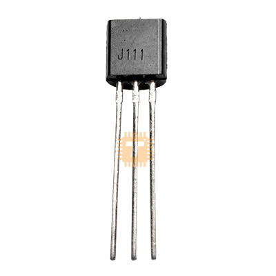
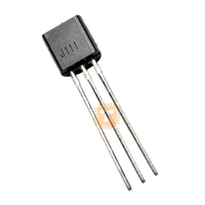
Original J111 N-Channel JFET Transistor TO-92 (DI0295) Products
| Name | Original J111 N-Channel JFET Transistor TO-92 |
| Code | DI0295 |
| Price | Rs.70.00 |
| In Stock | Yes |
| Package | THT |
Product Details
The J111 is an industry-standard, high-speed N-Channel Junction Field-Effect Transistor (JFET) encapsulated in a compact TO-92 plastic through-hole package. Specifically engineered for low-resistance analog switching, chopper circuits, commutators, and audio muting applications, the J111 features an exceptionally low on-state resistance (RDS(on) < 30>
Specifications
- Brand / Manufacturer: ON Semiconductor / Fairchild / InterFET / Industry Standard
- Part Number: J111
- Transistor Type: N-Channel Symmetrical Depletion-Mode JFET
- Drain-Source Voltage (VDS): 35V
- Drain-Gate Voltage (VDG): 35V
- Gate-Source Reverse Breakdown Voltage (VGSR): -35V
- Gate Current (IG): 50mA
- Zero-Gate-Voltage Drain Current (IDSS): Minimum 20mA (Typically 20mA to 100mA+ @ VDS = 15V, VGS = 0V)
- Gate-Source Cutoff Voltage (VGS(off)): -3.0V to -10.0V (at VDS = 15V, ID = 1.0µA)
- Static Drain-Source On-Resistance (RDS(on)): < 30>GS = 0V, ID = 1.0mA)
- Common-Source Input Capacitance (Ciss): Max 28pF (at VDS = 0V, VGS = -10V, f = 1.0MHz)
- Common-Source Reverse Transfer Capacitance (Crss): Max 5.0pF (at VDS = 0V, VGS = -10V, f = 1.0MHz)
- Turn-On Time (ton): Typically < 4>
- Turn-Off Time (toff): Typically < 25ns>
- Total Device Dissipation (PD): 350mW to 625mW (at TA = 25°C)
- Operating Junction & Storage Temperature: -55°C to +150°C
- Package / Case: TO-92 (3-Pin Through-Hole: Pin 1: Drain, Pin 2: Source, Pin 3: Gate)
Features
- Ultra-Low On-Resistance (RDS(on) ≤ 30Ω): Minimizes signal attenuation, insertion loss, and harmonic distortion in analog switching paths.
- Extremely Fast Switching Speeds: Fast nanosecond turn-on and turn-off response ensures clean switching without signal degradation or heavy delay.
- High Off-State Isolation: Sub-nanoampere gate and drain cutoff leakage currents ensure complete circuit isolation when turned off.
- Symmetrical Channel Geometry: Drain and Source terminals are fully interchangeable for bidirectional AC and DC signal switching.
- High Breakdown Margin (35V): Accommodates standard ±15V and ±12V analog operational amplifier signal swings without junction clipping.
Common Applications
- Analog Signal Switches & Multiplexers: High-speed, low-loss routing for audio signals, test signals, and instrumentation channels.
- Audio Muting & Anti-Pop Circuits: Pop-free audio output muting during power-up/power-down sequences in amplifiers and DACs.
- Choppers & Sample-and-Hold Stages: Fast charging and holding switches in precision data acquisition and ADC front-ends.
- Current Limiters & Constant Current Sources: Ultra-stable two-terminal constant current regulators when Gate is tied to Source.
- Voltage-Controlled Attenuators: Linear, low-distortion variable resistors (VCR) in AGC circuits and volume controls.
Usage Tips
- Pinout Identification: Looking at the flat marked front face of the TO-92 package with leads pointing downward, the standard pinout is Pin 1: Drain (D), Pin 2: Source (S), and Pin 3: Gate (G).
- Switching Control Voltage: Because the J111 is a depletion-mode device, it is fully ON when VGS = 0V. To ensure the switch is completely OFF, pull the Gate negative with respect to the source by at least -10V (or beyond the maximum negative peak of the analog AC signal being switched).
- Gate Drive Series Resistor / Diode: When driving the gate from standard logic or discrete transistors, place a series diode or 10kΩ resistor to prevent forward-biasing the Gate-Channel PN junction (VGS must not exceed +0.7V).
- Constant Current Diode Configuration: To use the J111 as a simple 2-terminal constant current regulator, tie the Gate (Pin 3) directly to the Source (Pin 2); the current flowing through will equal the saturated drain current (IDSS).
Sharing is caring, show love and share the product with your friends.
Featured


Add to Cart

Add to Cart

Add to Cart