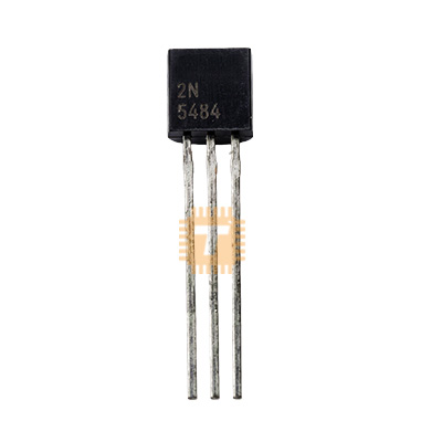
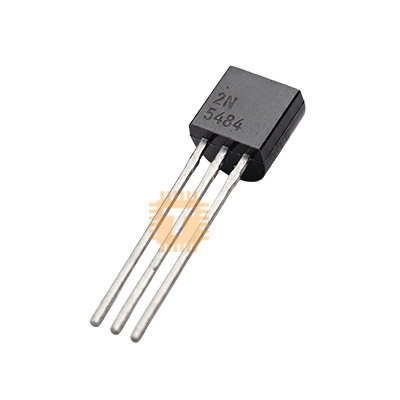
Original 2N5484 N-Channel JFET Transistor TO-92 (DI0293) Products
| Name | Original 2N5484 N-Channel JFET Transistor TO-92 |
| Code | DI0293 |
| Price | Rs.100.00 |
| In Stock | Yes |
| Package | THT |
Product Details
The 2N5484 is an industry-standard, high-frequency N-Channel Junction Field-Effect Transistor (JFET) encapsulated in a compact TO-92 plastic through-hole package. Engineered specifically for VHF/UHF amplifiers, RF mixers, oscillators, and low-noise input stages, the 2N5484 features high input impedance, very low noise figure, low cross-modulation distortion, and low inter-electrode capacitances. It is widely used in RF preamplifiers, analog switches, high-impedance buffer circuits, audio preamps, and laboratory instrumentation.
Specifications
- Brand / Manufacturer: Central Semiconductor / ON Semiconductor / Fairchild / Industry Standard
- Part Number: 2N5484
- Transistor Type: N-Channel Depletion-Mode RF JFET
- Drain-Source Voltage (VDS): 25V
- Drain-Gate Voltage (VDG): 25V
- Gate-Source Reverse Breakdown Voltage (VGSR): -25V
- Gate-Source Forward Voltage (VGSF): 0.5V
- Gate Current (IG): 10mA
- Zero-Gate-Voltage Drain Current (IDSS): 1.0mA to 5.0mA (at VDS = 15V, VGS = 0V)
- Gate-Source Cutoff Voltage (VGS(off)): -0.3V to -3.0V (at VDS = 15V, ID = 10nA)
- Forward Transconductance (|Yfs| / gfs): 3000µS to 6000µS (at VDS = 15V, VGS = 0V, f = 1.0kHz)
- Common-Source Input Capacitance (Ciss): Max 5.0pF (at VDS = 15V, VGS = 0V, f = 1.0MHz)
- Common-Source Reverse Transfer Capacitance (Crss): Max 1.0pF (at VDS = 15V, VGS = 0V, f = 1.0MHz)
- Noise Figure (NF): Approx. 2.0 dB (Typical at f = 100MHz) / Max 3.0 dB (at f = 400MHz)
- Total Device Dissipation (PD): 350mW (at TA = 25°C)
- Operating Junction & Storage Temperature: -55°C to +150°C
- Package / Case: TO-92 (3-Pin Through-Hole: Pin 1: Drain, Pin 2: Source, Pin 3: Gate)
Features
- Ultra-Low Noise Figure: Ensures clear signal reception and minimal noise contribution in sensitive RF front-end stages.
- High Input Impedance: Extremely high gate isolation prevents loading on tuned RF/audio tank circuits and sensor inputs.
- Very Low Feedback Capacitance (Crss < 1>
- Wide Dynamic Range: Depletion-mode planar design offers superior cross-modulation and intermodulation performance compared to standard BJTs.
- Compact TO-92 Packaging: Small footprint makes it easy to integrate into RF modules, breadboards, and legacy analog circuitry.
Common Applications
- VHF/UHF RF Preamplifiers: Low-noise front-end signal amplification in FM receivers, amateur radios, and scanners.
- High-Frequency Oscillators & Mixers: Local oscillator and active mixer circuits in communication transceivers.
- High-Impedance Audio Buffers: Input buffer stages for guitar pedals, piezo pickups, and condenser microphones.
- Analog Signal Switching: Low-distortion chopper and analog mute switching stages in audio equipment.
- Active Probes & Test Instruments: Ultra-high impedance signal tapping for oscilloscopes and frequency counters.
Usage Tips
- Pinout Identification: Looking at the flat face of the TO-92 package with leads pointing downward, the standard pinout is Pin 1: Drain (D), Pin 2: Source (S), and Pin 3: Gate (G). Note that in many symmetric JFET designs, Drain and Source can be electrically interchangeable, but adhering to the manufacturer layout ensures optimal noise and capacitance matching.
- Gate Biasing: Because the 2N5484 is a depletion-mode device, it is naturally ON when VGS = 0V; apply a negative voltage to the Gate relative to the Source (or use a source self-bias resistor bypassed with a capacitor) to set the desired quiescent drain current (ID).
- Gate Static Protection: Although more rugged than MOSFETs, JFET gates are sensitive to high reverse electrostatic voltages; handle with standard ESD precautions and place a high-value gate ground reference resistor (e.g., 1MΩ to 10MΩ).
- High-Frequency PCB Layout: Keep RF leads as short as possible and use a solid ground plane around the Gate and Drain nodes to minimize stray parasitic capacitance.
Sharing is caring, show love and share the product with your friends.
Featured


Add to Cart