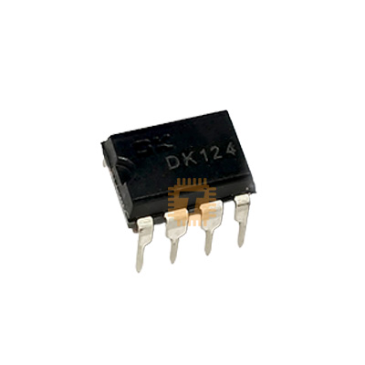
Original DK124 24W Switching Power Supply Controller (IC0355) Products
| Name | Original DK124 24W Switching Power Supply Controller |
| Code | IC0355 |
| Price | Rs.70.00 |
| In Stock | Yes |
Product Details
The Original DK124 24W Offline Switching Power Supply Controller is a high-performance, cost-effective AC-DC flyback switch-mode power supply (SMPS) integrated circuit manufactured by Dongke Semiconductor. Encapsulated in a standard DIP-8 through-hole package, it integrates a dedicated pulse-width modulation (PWM) controller, a 700V high-voltage power switching transistor, and an internal high-voltage constant-current startup circuit on a single monolithic die. Designed for price-sensitive isolated and non-isolated offline converter applications up to 24W, the DK124 utilizes a patented dynamic self-power supply architecture that eliminates the need for an auxiliary transformer bias winding and external startup resistors. It delivers high operating efficiency, built-in frequency jittering for low EMI noise, an internal 16ms soft-start circuit, and comprehensive protection against over-temperature, over-voltage, over-current, and output short circuits.
Specifications
- Part Number / Model: DK124 (Dongke Semiconductor Offline SMPS Series)
- Device Function: Integrated Offline AC-DC Flyback PWM Power Controller
- Package Type: DIP-8 (Dual In-Line 8-Pin Through-Hole, Plastic)
- Input AC Voltage Range: Universal 85V to 265V AC (50/60 Hz)
- Maximum Output Power Rating:
- 85V to 265V AC (Universal Input): Up to 12W – 18W (Enclosed adapter) / 24W (Open frame)
- 180V to 265V AC (High-Line Input): Up to 18W – 24W
- Integrated Power Transistor Breakdown Voltage (Vcol / Vds): 700V (Absolute Max: 780V)
- Peak Switch Current Limit (Ip): Typ. 1.3A / Max. 1.5A
- Nominal Switching Frequency: Typ. 65 kHz (61 kHz to 69 kHz with built-in frequency jittering)
- IC Operating Supply Voltage (Vcc): 4.65V to 5.25V DC (Internally self-regulated)
- Vcc Startup Threshold Voltage: Typ. 5.05V (4.75V to 5.35V)
- Vcc Restart / UVLO Voltage: Typ. 3.60V (3.30V to 3.90V)
- Vcc Over-Voltage Protection Threshold: Typ. 6.55V (6.25V to 6.85V)
- Internal Soft-Start Duration: Typ. 16 ms
- Leading Edge Blanking Time (LEB): Typ. 250 ns
- Minimum Turn-On Time: Typ. 500 ns
- Maximum PWM Duty Cycle: 70%
- Standby Power Consumption: < 240>
- Over-Temperature Protection (OTP) Threshold: Typ. 130°C (120°C to 140°C with auto-recovery)
- Total IC Power Dissipation (Pd): 1.0W (at Ta = 25°C)
- Operating Case Temperature (Tc): -20°C to +140°C
- Storage Temperature Range (Tstg): -55°C to +150°C
- Pinout Configuration:
- Pin 1: Ground (GND) - IC primary signal ground reference
- Pin 2: Ground (GND) - IC primary power ground reference
- Pin 3: Feedback (Fb) - Optocoupler feedback input pin
- Pin 4: Power Supply (Vcc) - External Vcc bypass capacitor connection
- Pin 5: Collector / Drain Output (OC) - High-voltage power switch terminal
- Pin 6: Collector / Drain Output (OC) - High-voltage power switch terminal
- Pin 7: Collector / Drain Output (OC) - High-voltage power switch terminal
- Pin 8: Collector / Drain Output (OC) - High-voltage power switch terminal
Features
- Integrated 700V Power Switch: Monolithic internal high-voltage switching transistor withstands severe line surges and simplifies secondary-side flyback converter topologies.
- Patented Dynamic Self-Powering Architecture: Generates internal operating voltage directly from the high-voltage collector pins during switching, completely eliminating the need for an auxiliary transformer bias winding, diode, and capacitor.
- Built-in High-Voltage Startup Circuit: Internal current source charges the Vcc bypass capacitor at power-up without requiring lossy external high-voltage bleeder startup resistors.
- Integrated 16ms Soft-Start: Linearly steps up primary peak current from 100mA to rated limits during startup, preventing transformer magnetic saturation and reducing stress on output rectifier diodes.
- Frequency Jittering for Low EMI: Sweeps switching frequency around 65 kHz to spread electromagnetic interference energy across adjacent bands, significantly reducing EMI filter component size and cost.
- Comprehensive Multi-Protection Suite: Includes cycle-by-cycle over-current protection (OCP), over-load protection (OLP), over-temperature protection (OTP with hysteresis), over-voltage clamping (OVP), and output short-circuit protection.
Common Applications
- AC-DC Power Adapters & Wall Chargers: 5V/2A, 12V/1.5A, and 12V/2A power bricks for routers, modems, and consumer electronics.
- Household Appliance Auxiliary Supplies: Standby power boards for air conditioners, washing machines, refrigerators, and induction cookers.
- Set-Top Boxes (STB) & Media Players: Multi-rail secondary flyback power supplies for satellite decoders and TV boxes.
- LED Lighting Drivers: Constant-current and constant-voltage offline LED drivers and lighting modules.
- Industrial Auxiliary & Standby Rails: Microcontroller power stages in smart meters, motor control units, and PLC power modules.
Usage Tips
- Vcc Capacitor Selection: Connect a high-quality 10µF to 47µF (typically 22µF / 16V) low-ESR electrolytic capacitor in parallel with a 100nF ceramic capacitor between Pin 4 (Vcc) and Pins 1/2 (GND) right next to the IC to ensure stable self-powering during dynamic load transients.
- Thermal PCB Heat-Sinking: Pins 5, 6, 7, and 8 (OC) act as the primary thermal dissipation path for the internal power switch. Connect all four OC pins together on the PCB to a wide, thick copper plane with thermal vias to keep junction temperatures well below the 130°C OTP threshold under full 24W loads.
- Primary RCD Snubber Clamping: Always place an RCD clamp circuit (fast recovery diode such as US1M/FR107, 1nF–2.2nF 1kV ceramic/film capacitor, and 68kΩ–100kΩ resistor) across the primary transformer winding to clamp leakage inductance voltage spikes below the 700V collector breakdown limit.
- Feedback Loop (Pin 3 Fb) Layout: Connect Pin 3 to the collector of the secondary-feedback optocoupler (e.g., PC817) with a 10nF ceramic filtering capacitor placed directly between Pin 3 and Pin 1 (GND) to suppress high-frequency noise from corrupting PWM duty cycle regulation.
- Transformer Design Guidance: Design the primary inductance (Lp) for discontinuous conduction mode (DCM) or continuous conduction mode (CCM) with peak primary current below 1.2A to avoid triggering the internal 1.3A cycle-by-cycle OCP limit during full load startup.
Sharing is caring, show love and share the product with your friends.
Featured

Add to Cart


Add to Cart