
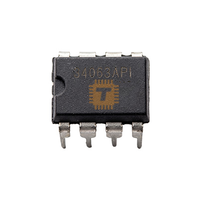
Original UCC37322 High Speed MOSFET Driver DIP-8 (IC0365) Products
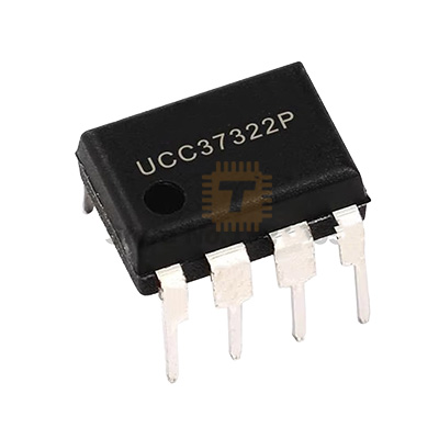
| Name | Original UCC37322 High Speed MOSFET Driver DIP-8 |
| Code | IC0365 |
| Price | Rs.530.00 |
| In Stock | Yes |
| Package | SMD |
Product Details
The Original UCC37322 High-Speed Non-Inverting MOSFET and IGBT Gate Driver IC is a high-performance, single-channel low-side gate driver manufactured by Texas Instruments. Encapsulated in a classic DIP-8 (PDIP-8) through-hole package, it delivers massive peak source and sink currents of up to 9.0A into large capacitive power MOSFET and IGBT gates. Utilizing Texas Instruments' TrueDrive™ compound bipolar and CMOS output architecture, the driver delivers maximum current capability right at the critical Miller plateau region during power switch transitions. Featuring fast 20ns rise and fall times, low propagation delays, and an integrated enable/disable function, the UCC37322 offers non-inverting drive control for high-efficiency switch-mode power supplies (SMPS), synchronous buck/boost stages, motor controllers, Tesla coil drivers, and high-frequency inverters.
Specifications
- Part Number / Model: UCC37322P / UCC37322 (Texas Instruments Marking: UCC37322P)
- Manufacturer: Texas Instruments
- Driver Configuration: Single-Channel Non-Inverting High-Speed Low-Side Gate Driver
- Output Architecture: TrueDrive™ Compound Bipolar and CMOS Output Stage
- Package Type: DIP-8
- Supply Voltage Range (VDD): 4.0V to 15.0V DC (Absolute Maximum: 16.0V DC)
- Peak Source / Sink Drive Current: Typ. ±9.0 A (at VDD = 14V)
- Output Rise Time (tr): Typ. 20 ns (with CL = 10,000 pF / 10 nF load)
- Output Fall Time (tf): Typ. 20 ns (with CL = 10,000 pF / 10 nF load)
- Propagation Delay Time: Typ. 25 ns (Input Falling) / 35 ns (Input Rising)
- Logic Input Compatibility: CMOS / TTL Compatible (Independent of VDD supply level; tolerates negative inputs down to -5V)
- Input Logic Thresholds:
- Logic High (VIH): Typ. 2.0V (Min. 2.2V)
- Logic Low (VIL): Typ. 1.1V (Max. 1.0V)
- Enable Control Function: Dedicated Active-High Enable Pin (ENBL) with Internal Pull-Up to VDD
- Operating Supply Current (Static): Typ. 0.3 mA to 1.0 mA
- Power Dissipation (Pd): Up to 350 mW to 650 mW (internally limited)
- Operating Temperature Range (Ta): Commercial / Extended 0°C to +70°C (Industrial rated up to +105°C)
- Storage Temperature Range (Tstg): -65°C to +150°C
- Pinout Configuration (DIP-8 - Standard Dual-In-Line):
- Pin 1: ENBL (Active-High Enable Input - Float or pull HIGH to enable output, pull LOW to force OUT LOW)
- Pin 2: IN (Non-Inverting Logic Control Input)
- Pin 3: NC (No Internal Connection)
- Pin 4: GND (Device Power & Signal Ground)
- Pin 5: GND (Device Power & Signal Ground - Internally tied to Pin 4)
- Pin 6: OUT (Non-Inverting Gate Drive Output - TrueDrive Stage)
- Pin 7: OUT (Non-Inverting Gate Drive Output - Internally paralleled with Pin 6)
- Pin 8: VDD (Power Supply Input, 4.0V to 15.0V)
Features
- 9.0A Peak Current TrueDrive™ Output: Combines paralleled Bipolar and MOSFET output devices to maintain maximum rated current during Miller plateau transitions, drastically reducing power switch switching losses.
- Non-Inverting High-Speed Logic: True non-inverting architecture means a logic HIGH at the input directly turns ON the power MOSFET/IGBT.
- VDD-Independent Logic Inputs: Directly compatible with 3.3V and 5.0V logic levels from microcontrollers (ESP32, STM32, Arduino, Raspberry Pi) without requiring external level-shifting buffers.
- Negative Input Voltage Tolerance: Logic input pins can safely handle negative transient swings down to -5V without latching up.
- Hardware Enable Pin (ENBL): Independent shutdown pin allows fast hardware fault shutdown, PWM blanking, or multi-driver sequencing.
- Prototyping-Friendly DIP-8 Package: Standard 0.1-inch (2.54mm) pitch through-hole package fits into breadboards, IC sockets, perfboards, and heavy-copper PCBs.
Common Applications
- High-Power Switch-Mode Power Supplies (SMPS): Primary and secondary low-side gate driving in Flyback, Forward, Half-Bridge, and Push-Pull converters.
- Synchronous Rectifier Drivers: High-current gate driving for low RDS(on) MOSFETs in synchronous buck/boost DC-DC regulators.
- Solid-State Tesla Coils (SSTC / DRSSTC) & Induction Heaters: High-frequency resonant switching stages requiring massive peak gate charging currents.
- Motor Drivers & H-Bridge Inverters: Low-side switching for high-power DC motor, stepper, and BLDC drive stages.
- Pulse Generators & Laser Diode Drivers: High-speed current pulse generation with sub-nanosecond jitter.
Usage Tips
- Non-Inverting Logic Configuration: Because the UCC37322 is **non-inverting**, driving Pin 2 (IN) HIGH drives Pin 6/7 (OUT) to VDD. When Pin 2 is LOW, OUT is pulled securely to GND.
- Supply Rail Decoupling (Critical): Rapidly charging large gates at 9A generates severe current pulses. Place a **1.0µF to 4.7µF low-ESR ceramic capacitor in parallel with a 10µF to 22µF electrolytic/tantalum capacitor directly across Pin 8 (VDD) and Pins 4/5 (GND)** with minimal trace length.
- Damping Gate Resistor: Keep the gate drive loop between Pin 6/7 (OUT) and the external MOSFET gate/source pins as short as possible. Use a small series resistor (e.g., 2.2Ω to 10Ω) to dampen high-frequency ringing caused by lead inductance.
- Paralleling Pins: On your PCB, always bridge **Pin 6 with Pin 7 (OUT)** and bridge **Pin 4 with Pin 5 (GND)** to minimize package parasitic lead inductance and share high-current discharge paths.
- Enable Pin Connection: If hardware enable control is not required, tie Pin 1 (ENBL) directly to Pin 8 (VDD) to prevent floating noise triggers.
Sharing is caring, show love and share the product with your friends.
Featured


Add to Cart


Other Products

Add to Cart
