Original FCH190N65F 650V 20.6A N-Channel MOSFET TO-247 (DI0300) Products
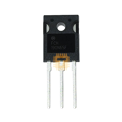
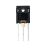
| Name | Original FCH190N65F 650V 20.6A N-Channel MOSFET TO-247 |
| Code | DI0300 |
| Price | Rs.1,560.00 |
| In Stock | Yes |
| Package | TO-247 |
Product Details
The Original FCH190N65F 650V 20.6A N-Channel Super-Junction Power MOSFET is a high-voltage, fast-recovery power transistor engineered using ON Semiconductor / Fairchild SuperFET II FRFET technology. Housed in a heavy-duty TO-247 through-hole power package, this device features an exceptionally low on-state resistance (Rds(on)) of 190mΩ, high dv/dt ruggedness, and an integrated fast-recovery body diode with low reverse recovery charge (Qrr). It is specifically optimized for high-efficiency resonant topologies, solar inverters, telecom server power supplies, industrial motor drives, and high-frequency switch-mode power systems.
Specifications
- Part Number / Model: FCH190N65F (SuperFET II FRFET Series / ON Semiconductor - Fairchild)
- Transistor Type: N-Channel Super-Junction Power MOSFET
- Package Type: TO-247
- Drain-Source Breakdown Voltage (Vds): 650V (at Tj = 25°C) / 700V (at Tj = 150°C)
- Gate-Source Voltage (Vgs): ±20V DC (±30V AC peak)
- Continuous Drain Current (Id):
- 20.6A (at Tc = 25°C)
- 13.1A (at Tc = 100°C)
- Pulsed Drain Current (Idm): 61.8A Peak
- Static Drain-Source On-Resistance (Rds(on)): Typ. 160mΩ / Max. 190mΩ (at Vgs = 10V, Id = 10.3A)
- Body Diode Reverse Recovery Time (trr): Typ. 100ns to 130ns (Ultra-Fast FRFET Recovery)
- Body Diode Reverse Recovery Charge (Qrr): Typ. 460nC to 550nC
- Gate Threshold Voltage (Vgs(th)): 3.0V to 5.0V (at Vds = Vgs, Id = 2.0mA)
- Total Gate Charge (Qg): Typ. 57nC (at Vds = 520V, Id = 10.3A, Vgs = 10V)
- Input Capacitance (Ciss): Typ. 2380pF (at Vds = 100V, f = 1MHz)
- Total Power Dissipation (Pd): 208W (at Tc = 25°C)
- Operating Junction & Storage Temperature: -55°C to +150°C
- Pinout Configuration: Pin 1: Gate (G), Pin 2: Drain (D), Pin 3: Source (S), Tab: Drain (D)
Features
- SuperFET II FRFET Technology: Combines ultra-low conduction losses with high-speed switching and exceptional avalanche ruggedness.
- Integrated Fast-Recovery Body Diode: Features an ultra-fast reverse recovery diode that significantly reduces diode recovery dv/dt and turn-on losses in half-bridge and full-bridge bridge configurations.
- High Breakdown Safety Margin: 650V rated breakdown voltage (rising to 700V at operating temperatures) provides ample headroom for AC mains transient surges.
- Low Gate Charge (Qg): Reduces gate drive power requirements and allows high-frequency PWM operation with minimal driver heating.
- Robust TO-247 Package: Large thermal surface area enables efficient heat dissipation and secure bolting to chassis heatsinks for sustained high-wattage operation.
Common Applications
- LLC Resonant Half-Bridge / Full-Bridge Converters: Primary switching stage for high-efficiency server power supplies and telecom rectifiers.
- Solar & Renewable Energy Inverters: High-voltage DC-DC boost and DC-AC inversion bridge circuits.
- Uninterruptible Power Supplies (UPS): High-efficiency power conversion stages for online/standby industrial UPS systems.
- Power Factor Correction (PFC): Continuous Conduction Mode (CCM) boost PFC stages in high-wattage power supplies.
- Industrial Motor Drives & Welding Inverters: Primary bridge switching in industrial welders, plasma cutters, and frequency drives.
Usage Tips
- Heatsink Mounting & Insulation: Always mount with a thermally conductive silicone pad (such as TO-247/TO-3P size) and an insulating screw washer if the heatsink is electrically connected to ground or chassis.
- Gate Drive Circuitry: Drive with a standard 10V to 15V gate voltage to guarantee full saturation and achieve the lowest Rds(on) conduction resistance.
- Gate Damping: Place a series gate resistor (typically 4.7Ω to 22Ω) close to Pin 1 (Gate) to suppress parasitic ringing and voltage spikes caused by PCB trace inductance.
- Decoupling & Snubbers: In hard-switching applications, use high-voltage ceramic bypass capacitors and RC snubber networks across the drain-source terminals to absorb high-voltage inductive switching spikes.
Sharing is caring, show love and share the product with your friends.
Featured


Add to Cart

Add to Cart
Other Products
Add to Cart