Original IR2104S Half Bridge Driver SOIC-8 (DI0298) Products
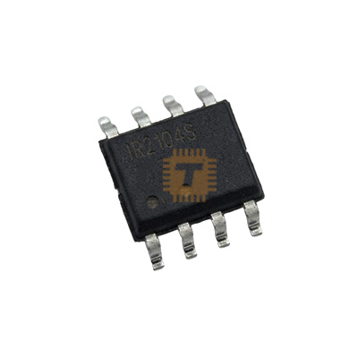
| Name | Original IR2104S Half Bridge Driver SOIC-8 |
| Code | DI0298 |
| Price | Rs.190.00 |
| In Stock | Yes |
| Package | DBS |
Product Details
The Original IR2104S High and Low Side Driver IC is a high-voltage, high-speed power MOSFET and IGBT half-bridge driver housed in a compact SOIC-8 surface-mount package. Featuring proprietary high-voltage level-shifting technology, an internal deadtime generator, and a cross-conduction prevention circuit, the IR2104S allows low-voltage logic signals (3.3V, 5V, or 15V) to safely control high-voltage half-bridge switching configurations up to 600V. It is widely used in DC-DC buck/boost converters, brushless DC (BLDC) motor drivers, Class-D audio amplifiers, pure sine wave inverters, and switch-mode power supplies.
Specifications
- Part Number / Model: IR2104S / IR2104STR (Infineon / International Rectifier)
- IC Function: High-Voltage, High-Speed Half-Bridge Gate Driver
- Package Type: SOIC-8
- High-Side Floating Offset Voltage (Voffset / Vb): Up to +600V DC Max
- Gate Drive Supply Voltage (Vcc): 10V to 20V DC
- Peak Output Source Current (Io+): Typ. 130mA (Min. 60mA)
- Peak Output Sink Current (Io-): Typ. 270mA (Min. 120mA)
- Logic Input Compatibility: 3.3V, 5V, and 15V CMOS / LSTTL Logic Levels
- Input Threshold Voltages: Vih = 2.7V (Min), Vil = 0.8V (Max)
- Internal Deadtime (DT): Typ. 520ns (Prevents shoot-through currents)
- Turn-On Propagation Delay (ton): Typ. 680ns
- Turn-Off Propagation Delay (toff): Typ. 150ns
- Rise Time (tr) / Fall Time (tf): Typ. 100ns / Typ. 50ns (with 1000pF load)
- Operating Junction Temperature (Tj): -40°C to +150°C
- Pinout Configuration:
- Pin 1: IN (Logic Input for High & Low Side Gate Driver Outputs)
- Pin 2: SD (Shutdown Control, Active Low)
- Pin 3: VCC (Low-Side and Logic Fixed Supply Voltage)
- Pin 4: COM (Low-Side Return / Power Ground)
- Pin 5: LO (Low-Side Gate Drive Output)
- Pin 6: VS (High-Side Floating Supply Offset / Half-Bridge Midpoint)
- Pin 7: HO (High-Side Gate Drive Output)
- Pin 8: VB (High-Side Floating Supply / Bootstrap Voltage)
Features
- High-Voltage Bootstrap Operation: Fully operational up to +600V, with floating channel design immune to high dV/dt transient noise.
- Built-in Shoot-Through Protection: Matched propagation delays and an internal 520ns deadtime prevent simultaneous conduction of high-side and low-side MOSFETs/IGBTs.
- Integrated Shutdown Control (SD): Allows instant shutdown of both gate drive outputs via microcontroller logic during overcurrent or fault conditions.
- Low-Voltage Logic Interface: Direct interface to standard 3.3V and 5V microcontroller I/O pins (Arduino, ESP32, STM32) without external level-shifting buffers.
- Under-Voltage Lockout (UVLO): Integrated UVLO protection on the VCC supply prevents power MOSFETs from operating in linear, high-heat dissipation regions during low gate-drive supply states.
Common Applications
- BLDC & Stepper Motor Drives: Driving high-side and low-side N-channel MOSFET bridges in 3-phase and H-bridge motor controllers.
- Pure Sine Wave & Solar Inverters: Output bridge switching stages in 12V/24V/48V to 230VAC power inverters.
- Synchronous DC-DC Buck / Boost Converters: High-efficiency voltage regulator modules replacing passive freewheeling diodes with active MOSFETs.
- Class-D Audio Power Amplifiers: High-speed output stage switching for compact, high-efficiency digital audio amplifiers.
- Induction Heating & Wireless Power: High-frequency half-bridge resonant tank drivers.
Usage Tips
- Bootstrap Diode Selection: Use an ultra-fast recovery diode (such as UF4007, US1M, or ES1J) between VCC and VB to ensure fast charging of the bootstrap capacitor with minimal reverse recovery losses.
- Bootstrap Capacitor Sizing: Place a high-quality 0.1µF to 1.0µF low-ESR ceramic capacitor directly between Pin 8 (VB) and Pin 6 (VS) with minimal PCB trace length.
- Gate Resistors: Place individual series gate damping resistors (typically 10Ω to 47Ω) between HO/LO and the respective MOSFET gates to prevent high-frequency ringing and parasitic oscillations.
- Grounding Separation: Separate sensitive signal ground (microcontroller GND) from heavy high-current switching ground paths, tying them together at a single star-ground point near Pin 4 (COM).
Sharing is caring, show love and share the product with your friends.
Featured


Add to Cart

Add to Cart

Other Products
Add to Cart