Original SCTW100N65G2AG 650V 100A Silicon Carbide Power MOSFET Hip247 TO-247 (DI0301) Products
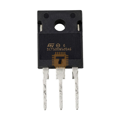
| Name | Original SCTW100N65G2AG 650V 100A Silicon Carbide Power MOSFET Hip247 TO-247 |
| Code | DI0301 |
| Price | Rs.3,160.00 |
| In Stock | Yes |
| Package | Hip247 |
Product Details
The Original SCTW100N65G2AG 650V 100A Silicon Carbide (SiC) Power MOSFET is a cutting-edge, automotive-grade (AEC-Q101 qualified) wide bandgap power transistor manufactured by STMicroelectronics using 2nd Generation SiC MOSFET technology. Housed in a thermally optimized HiP247 (TO-247) package, this device delivers an ultra-low on-state resistance (Rds(on)) of just 20mΩ, virtually zero reverse recovery charge, and exceptional switching performance up to 200°C junction temperatures. It is specifically designed for ultra-high-efficiency electric vehicle (EV) traction inverters, high-power DC-DC converters, EV fast chargers, solar PV inverters, and high-density industrial power systems.
Specifications
- Part Number / Model: SCTW100N65G2AG (Gen 2 SiC MOSFET Series / STMicroelectronics)
- Transistor Type: N-Channel Silicon Carbide (SiC) Power MOSFET
- Qualification: AEC-Q101 Qualified (Automotive Grade)
- Package Type: TO-247
- Drain-Source Breakdown Voltage (Vds): 650V
- Gate-Source Voltage (Vgs): -10V to +22V (Recommended Turn-ON: +18V to +20V, Turn-OFF: 0V to -4V)
- Continuous Drain Current (Id):
- 100A (at Tc = 25°C)
- 70A to 75A (at Tc = 100°C)
- Pulsed Drain Current (Idm): 250A Peak
- Static Drain-Source On-Resistance (Rds(on)): Typ. 20mΩ / Max. 26mΩ (at Vgs = 18V, Id = 50A, Tj = 25°C)
- Total Gate Charge (Qg): Typ. 120nC to 140nC
- Input Capacitance (Ciss): Typ. 3200pF (at Vds = 400V, f = 1MHz)
- Reverse Recovery Charge (Qrr): Ultra-Low (~120nC SiC Body Diode)
- Reverse Recovery Time (trr): Ultra-Fast (≤ 25ns)
- Total Power Dissipation (Pd): 450W (at Tc = 25°C)
- Operating Junction Temperature (Tj): -55°C to +200°C (Extended High-Temperature Capability)
- Thermal Resistance, Junction to Case (Rth(j-c)): ~0.35°C/W
- Pinout Configuration: Pin 1: Gate (G), Pin 2: Drain (D), Pin 3: Source (S), Tab: Drain (D)
Features
- Wide Bandgap Silicon Carbide (SiC) Material: Operates at significantly higher switching frequencies, higher voltages, and higher temperatures than standard silicon devices with vastly lower switching losses.
- Ultra-Low 20mΩ On-Resistance: Extremely low conduction losses that remain stable across high temperatures, maximizing overall system efficiency up to 99%+.
- Near-Zero Body Diode Reverse Recovery: Virtually eliminates diode recovery losses and peak current overshoot in hard-switched bridge configurations.
- Extended 200°C Operating Temperature: Withstands extreme operating conditions, significantly reducing heatsink size and cooling requirements.
- High-Speed Switching Capability: Enables reduction in size, weight, and cost of passive magnetic components (transformers, inductors) and capacitors by operating at multi-hundred-kilohertz frequencies.
Common Applications
- Electric Vehicle (EV / HEV) Systems: Main traction inverters, on-board chargers (OBC), and high-voltage DC-DC battery converters.
- EV Fast Charging Stations: Ultra-high-power DC fast-charging power modules (Level 3 / CCS chargers).
- Solar & Renewable Energy: High-efficiency central string solar inverters, energy storage systems (ESS), and microgrid converters.
- High-Density Server & Telecom Power: Power Factor Correction (Totem-Pole PFC) and LLC resonant converters in data center power supplies.
- Industrial Motor Drives & Induction Heating: High-frequency resonant inverters, welding machines, and high-efficiency variable-frequency drives (VFD).
Usage Tips
- Gate Driver Selection: Use a dedicated SiC isolated gate driver (such as STGAP series or UCC217xx) capable of providing +18V to +20V for turn-on and -2V to -5V negative gate bias for reliable turn-off to prevent parasitic turn-on caused by high dV/dt.
- Kelvin Connection & PCB Layout: Minimize gate-source loop inductance by placing the gate driver IC as close to the transistor pins as possible and routing gate and source return traces tightly together.
- Heatsink & Thermal Management: Mount the HiP247 tab securely to a high-performance copper/aluminum heatsink with high-conductivity thermal interface material (such as 6.0 W/m·K+ thermal pads or paste) to leverage the 450W power capability.
- High-Frequency Snubbers: Include high-voltage, low-inductance ceramic bypass capacitors directly across the DC bus near the MOSFET drain-source pins to suppress rapid voltage transients during nanosecond-speed switching.
Sharing is caring, show love and share the product with your friends.
Featured


Add to Cart

Add to Cart
Add to Cart