Original TLV9062 Dual Op-Amp IC SOIC-8 (IC0333) Products
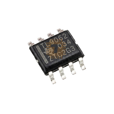
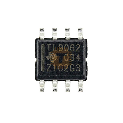
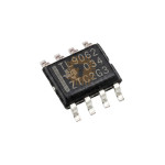
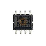
| Name | Original TLV9062 Dual Op-Amp IC SOIC-8 |
| Code | IC0333 |
| Price | Rs.70.00 |
| In Stock | Yes |
| Package | SMD |
Product Details
The TLV9062 is a high-performance, dual-channel operational amplifier designed for low-voltage (1.8V to 5.5V) applications. It is specifically optimized for cost-sensitive projects that require a high bandwidth-to-power ratio. With its rail-to-rail input and output (RRIO) capabilities, it is a superior choice for modern battery-powered electronics where maximizing signal dynamic range is critical.
Specifications
- Supply Voltage: 1.8V to 5.5V (Single Supply)
- Gain Bandwidth Product (GBW): 10MHz
- Slew Rate: 6.5V / us
- Low Quiescent Current: 538uA per channel
- Low Input Bias Current: 0.5pA (Typical)
- Operating Temperature: -40°C to 125°C
- Package: SOIC-8 (Surface Mount)
Features
- Rail-to-Rail I/O: The output can swing very close to the supply rails (typically within millivolts), ensuring you don't lose signal resolution in 3.3V or 5V systems.
- EMI/RFI Filtering: Includes integrated internal filters to reduce sensitivity to electromagnetic interference, making it stable in environments with WiFi or Bluetooth signals.
- High Precision: Despite being a "general purpose" part, it offers low offset voltage and very low input bias current thanks to its CMOS construction.
- Unity-Gain Stable: Can be used as a buffer/voltage follower without additional compensation components.
- Robust ESD Protection: Features internal ESD protection reaching 2kV (HBM), increasing durability during assembly.
Common Applications
- Battery-Powered Instruments: Handheld multimeters, scales, and portable medical devices.
- Sensor Signal Conditioning: Interfacing with photodiodes, PIR sensors, and high-impedance transducers.
- Active Filtering: Designing compact, high-order low-pass or band-pass filters for audio or data.
- Motor Control Feedback: Low-side current sensing and position feedback loops.
- Audio Pre-amplification: High-bandwidth performance suitable for consumer audio signals.
Usage Tips
- Decoupling: To maintain the 10MHz bandwidth performance, place a 0.1uF ceramic bypass capacitor directly between pins 8 (V+) and 4 (GND).
- Input Impedance: Because the input bias current is almost zero (0.5pA), you can use very high-value resistors (megohms) in your feedback loops without introducing significant offset errors.
- Logic Levels: If you are using this with a microcontroller, ensure the V+ matches the MCU's logic level (e.g., 3.3V) to keep signals within the ADC's range.
- Soldering: As an SMD component, ensure the PCB footprint matches the "Small Outline Integrated Circuit" (SOIC) standard. Pin 1 is typically marked with a dot or a beveled edge on the plastic body.
Sharing is caring, show love and share the product with your friends.
Featured

Add to Cart


Other Products
Add to Cart