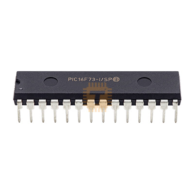
Original Microchip PIC16F73 DIP-28 (MC0003) Products
| Name | Original Microchip PIC16F73 DIP-28 |
| Code | MC0003 |
| Price | Rs.920.00 |
| In Stock | Yes |
| Package | SOIC-28 |
Product Details
The Original Microchip PIC16F73 8-Bit Flash Microcontroller is a classic, robust, and versatile 28-pin MCU manufactured by Microchip Technology. Encapsulated in an industry-standard 0.300-inch skinny DIP-28 (PDIP-28 / SPDIP-28) through-hole package, it is powered by an efficient mid-range 8-bit PIC RISC core operating at speeds up to 20 MHz. The PIC16F73 integrates a comprehensive set of hardware peripherals, including a 5-channel 8-bit Analog-to-Digital Converter (ADC), two Capture/Compare/PWM (CCP) modules, three hardware timers, a full-duplex Addressable USART, and a Master Synchronous Serial Port (MSSP) supporting SPI and I2C modes. Renowned for its high noise immunity, wide supply voltage operating window, and 25mA high-current sink/source I/O pins, the PIC16F73 is widely utilized in industrial motor controllers, UPS and pure sine wave inverters, smart battery chargers, power management systems, automotive subsystems, and embedded development projects.
Specifications
- Part Number / Model: PIC16F73-I/SP / PIC16F73 (Industrial Temperature Grade, Skinny DIP)
- Manufacturer: Microchip Technology
- Core Architecture: Mid-Range 8-Bit PIC RISC Core (35 Single-Word Instructions)
- Package Type: DIP-28
- Operating Voltage Range (VDD): 2.0V to 5.5V DC (Full 20 MHz speed rated from 4.0V to 5.5V DC)
- Maximum CPU Clock Speed: Up to 20 MHz (200 ns instruction execution cycle time at 20 MHz)
- Clock Sources: External Quartz Crystal, Ceramic Resonator, or RC Oscillator via OSC1/OSC2 pins
- Program Memory (Flash): 7.0 KB (4,096 Words Flash Program Memory, 1,000 erase/write cycles)
- Data SRAM: 192 Bytes
- General Purpose I/O (GPIO): 22 User I/O Pins across Port A, Port B, and Port C (with 25mA sink/source per pin)
- Analog-to-Digital Converter (ADC): 8-Bit Successive Approximation ADC with 5 Multiplexed Input Channels (AN0 to AN4)
- Capture / Compare / PWM (CCP) Modules: 2 Independent CCP Modules (10-Bit PWM Resolution, up to 20 kHz+ switching)
- Hardware Timers:
- Timer0: 8-Bit Timer/Counter with 8-bit software-programmable prescaler
- Timer1: 16-Bit Timer/Counter with external crystal/clock oscillator capability
- Timer2: 8-Bit Timer with 8-bit Period Register (PR2), prescaler, and postscaler
- Serial Communication Peripherals:
- 1x Addressable USART (Hardware Full-Duplex UART with 9-bit address detection support)
- 1x MSSP (Master Synchronous Serial Port supporting 3-wire SPI Master/Slave and I2C Slave/Master modes)
- Hardware Interrupt Sources: 11 Independent Interrupt Sources (External INT pin, TMR overflows, CCP, USART, ADC, etc.)
- Power-On Features: Power-on Reset (POR), Power-up Timer (PWRT), Oscillator Start-up Timer (OST), and Watchdog Timer (WDT)
- Operating Ambient Temperature (TA): -40°C to +85°C (Industrial Grade)
- Storage Temperature Range (Tstg): -65°C to +150°C
- Pinout Configuration (SPDIP-28):
- Pin 1: MCLR / VPP (Active-Low Master Clear Reset / High-Voltage Programming Voltage)
- Pin 2: RA0 / AN0 (Port A0 / ADC Channel 0)
- Pin 3: RA1 / AN1 (Port A1 / ADC Channel 1)
- Pin 4: RA2 / AN2 (Port A2 / ADC Channel 2)
- Pin 5: RA3 / AN3 / VREF (Port A3 / ADC Channel 3 / External Voltage Reference Input)
- Pin 6: RA4 / T0CKI (Port A4 / Timer0 External Clock Input - Open-Drain Output)
- Pin 7: RA5 / AN4 / SS (Port A5 / ADC Channel 4 / SPI Slave Select)
- Pin 8: VSS (Digital Ground / 0V Reference)
- Pin 9: OSC1 / CLKIN (Main Oscillator Crystal Input / External Clock)
- Pin 10: OSC2 / CLKOUT (Main Oscillator Crystal Output / Clock Output)
- Pin 11: RC0 / T1OSO / T1CKI (Port C0 / Timer1 Oscillator Output / Timer1 Clock Input)
- Pin 12: RC1 / T1OSI / CCP2 (Port C1 / Timer1 Oscillator Input / CCP2 Capture, Compare, PWM)
- Pin 13: RC2 / CCP1 (Port C2 / CCP1 Capture, Compare, PWM)
- Pin 14: RC3 / SCK / SCL (Port C3 / SPI Clock / I2C Clock)
- Pin 15: RC4 / SDI / SDA (Port C4 / SPI Data In / I2C Data)
- Pin 16: RC5 / SDO (Port C5 / SPI Data Out)
- Pin 17: RC6 / TX / CK (Port C6 / USART Asynchronous Transmit / Synchronous Clock)
- Pin 18: RC7 / RX / DT (Port C7 / USART Asynchronous Receive / Synchronous Data)
- Pin 19: VSS (Digital Ground / 0V Reference - Internally Connected)
- Pin 20: VDD (Positive Power Supply Input, +2.0V to +5.5V)
- Pin 21: RB0 / INT (Port B0 / External Hardware Interrupt Input)
- Pin 22: RB1 (Port B1 General Purpose I/O)
- Pin 23: RB2 (Port B2 General Purpose I/O)
- Pin 24: RB3 / PGM (Port B3 / Low-Voltage In-Circuit Serial Programming Enable)
- Pin 25: RB4 (Port B4 General Purpose I/O / Interrupt-on-Change)
- Pin 26: RB5 (Port B5 General Purpose I/O / Interrupt-on-Change)
- Pin 27: RB6 / PGC (Port B6 / In-Circuit Serial Programming Clock / Interrupt-on-Change)
- Pin 28: RB7 / PGD (Port B7 / In-Circuit Serial Programming Data / Interrupt-on-Change)
Features
- Dual 10-Bit Hardware CCP Modules: Built-in CCP1 and CCP2 modules allow precise PWM generation, hardware frequency measurement, and pulse timing without placing software timing burdens on the CPU.
- High-Drive 25mA I/O Ports: Every standard I/O pin can source and sink up to 25mA directly, allowing direct control of indicator LEDs, optocouplers, small relays, and logic gates.
- Hardware Serial USART & MSSP: Hardware UART (TX/RX) alongside simultaneous hardware SPI / I2C serial communications enables multi-device networking, RS-485 Modbus telemetry, and peripheral interfacing.
- High Noise Immunity: Engineered for harsh industrial environments, featuring high ESD resistance, Brown-out Reset (BOR), and a built-in Watchdog Timer (WDT) with an independent on-chip RC oscillator.
- Prototyping-Friendly 0.300-Inch SPDIP-28 Package: Slim DIP footprint fits standard breadboards, narrow 28-pin DIP sockets, and single/double-sided through-hole PCBs.
Common Applications
- Power Inverters & UPS Systems: PWM generation, voltage regulation, battery charging algorithms, and fault monitoring in modified and pure sine wave inverters.
- Industrial Motor Controllers & Drivers: Variable speed driving, soft-start regulation, and tachometer feedback for DC motors, fans, and pumps.
- Smart Battery Chargers: Multi-stage CC/CV battery management for Lead-Acid, NiCd/NiMH, and Lithium-based systems.
- Security & Access Control Systems: Keypad scanning, relay switching, serial RS-485 communication, and LCD front-panel management.
- DIY Robotics & Embedded Projects: Core controller for robotics rovers, sensor sampling arrays, and custom embedded systems.
Usage Tips
- In-Circuit Serial Programming (ICSP): For flashing and debugging with Microchip PICkit (PICkit 3, 4, 5) or standard ICSP programmers, connect:
- VPP/MCLR to Pin 1
- VDD (+5.0V) to Pin 20
- VSS (GND) to Pin 8 and Pin 19
- PGD / ICSPDAT to Pin 28 (RB7)
- PGC / ICSPCLK to Pin 27 (RB6)
- (If using High-Voltage ICSP, pull Pin 24 / RB3 / PGM low through a 10kΩ resistor or disable LVP in configuration words).
- Power Supply Decoupling: Place a **0.1µF (100nF) ceramic capacitor** as close as possible across Pin 20 (VDD) and Pin 19 (VSS), and connect Pin 8 (VSS) directly to your common ground plane to minimize switching noise during high-speed ADC sampling.
- MCLR Reset Circuit: Connect Pin 1 (MCLR) to VDD through a **10kΩ pull-up resistor** in series with a 100Ω damping resistor. For noisy environments, add a 100nF filter capacitor to ground at the junction (ensure ICSP programming lines are isolated during programming).
- Oscillator Crystal Loading: When using an external quartz crystal (e.g., 4 MHz, 8 MHz, 16 MHz, or 20 MHz) between Pin 9 (OSC1) and Pin 10 (OSC2), connect two **15pF to 22pF ceramic capacitors** from each crystal pin to ground, and select the appropriate oscillator mode (XT or HS) in the device configuration fuses.
- Port A Digital / Analog Configuration (ADCON1): By default at startup, Port A pins (RA0–RA5) power up as analog inputs. To use them as general-purpose digital I/O, you must explicitly configure the **ADCON1 register** (e.g., set `ADCON1 = 0x06` or `0x07` depending on the desired analog/digital split).
- Port A4 Open-Drain Output: Note that Pin 6 (RA4/T0CKI) is an **open-drain output**. When configured as a digital output, it requires an external pull-up resistor (e.g., 4.7kΩ to 10kΩ) connected to VDD to pull the pin HIGH.
Sharing is caring, show love and share the product with your friends.
Featured

Add to Cart


Other Products

Add to Cart