Original MUR3040PT Ultra-Fast Recovery Diode TO-247 (DI0284) Products
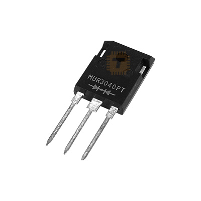
| Name | Original MUR3040PT Ultra-Fast Recovery Diode TO-247 |
| Code | DI0284 |
| Price | Rs.500.00 |
| In Stock | Yes |
| Package | THT |
Product Details
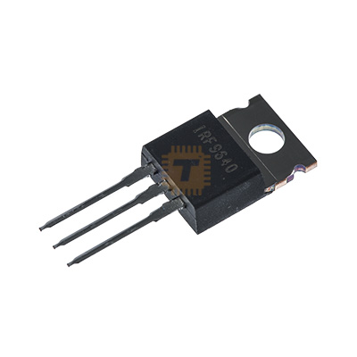
The MUR3040PT is a dual-chip, center-tap ultra-fast recovery power rectifier diode housed in a heavy-duty TO-247 (TO-218 / TO-3P compatible) through-hole package. Engineered specifically for high-efficiency, medium-to-high voltage switch-mode power conversion, the MUR3040PT features a repetitive peak reverse voltage rating of 400V, a total continuous forward current capacity of 30A (15A per diode leg), low forward voltage drop, and an ultra-fast reverse recovery time (trr) of 60ns. It is widely used in high-frequency switch-mode power supplies (SMPS), solar inverters, DC-DC step-down/boost converters, high-power battery chargers, and inductive freewheeling clamp circuits.
Specifications
- Brand / Manufacturer: ON Semiconductor / Fairchild / Vishay / Industry Standard
- Part Number / Marking: MUR3040PT / U3040PT
- Diode Configuration: Dual Common Cathode (Center Tap)
- Maximum Repetitive Peak Reverse Voltage (VRRM): 400V
- Working Peak Reverse Voltage (VRWM): 400V
- Maximum DC Blocking Voltage (VR): 400V
- Average Rectified Forward Current (IF(AV)): 30A Total (15A per Diode Leg at TC = 150°C)
- Non-Repetitive Peak Forward Surge Current (IFSM): 150A to 200A (8.3ms half sine-wave per leg)
- Maximum Instantaneous Forward Voltage (VF): 1.25V (at IF = 15A, TC = 25°C) / 1.12V (at IF = 15A, TC = 150°C)
- Maximum Reverse Recovery Time (trr): 60ns (at IF = 1.0A, di/dt = 50A/µs)
- Maximum Reverse Leakage Current (IR): 10µA @ TJ = 25°C / 1.0mA @ TJ = 150°C
- Operating Junction & Storage Temperature Range: -65°C to +175°C
- Thermal Resistance, Junction-to-Case (RθJC): 1.5°C/W per diode leg
- Package / Case: TO-247 / SOT-93 (TO-218) (Pin 1: Anode 1, Pin 2: Common Cathode / Tab, Pin 3: Anode 2)
Features
- Ultra-Fast 60ns Switching Speed: Substantially reduces reverse recovery losses and high-frequency switching noise in fast PWM power converters.
- Optimized 400V Blocking Voltage: Ideal voltage rating for intermediate-voltage offline power supplies and secondary bridge rectification.
- Dual Center-Tap Configuration: Combines two matched 15A diode legs with a shared cathode to simplify full-wave secondary rectification circuits and reduce component count.
- High Junction Operating Temperature (175°C): Delivers excellent thermal stability, reliability, and safe operating margins in elevated ambient temperature enclosures.
- High-Temperature Glass Passivated Junction: Ensures minimal reverse leakage and robust avalanche withstand capability over long operating lifetimes.
- High-Thermal TO-247 Package: Large copper baseplate provides direct heatsink mounting for superior thermal management under heavy continuous current loads.
Common Applications
- Switch-Mode Power Supplies (SMPS): High-frequency center-tap output rectification in telecom power supplies, server units, and ATX power supplies.
- Solar Inverters & UPS Systems: Secondary high-frequency output rectification and energy recycling in renewable energy systems.
- High-Power DC-DC Converters: Catch/freewheeling diode stages in industrial buck, boost, and bridge topologies.
- Industrial Battery Chargers: Fast rectification stages in multi-stage lead-acid and lithium battery charging equipment.
- Inductive Load Clamping: High-speed freewheeling protection across inductive motors, large solenoids, and magnetic actuators.
Usage Tips
- Heatsinking Requirement: Always fasten the TO-247 package to an adequately dimensioned aluminum heatsink with thermal paste. If the heatsink is electrically grounded, use a silicone/mica insulation sheet and shoulder washer (as Pin 2 and the mounting tab are tied to the Common Cathode).
- Single 30A Diode Configuration: To utilize the full 30A continuous capacity in a single-phase circuit, connect Pin 1 (Anode 1) and Pin 3 (Anode 2) together in parallel on the PCB.
- RC Snubber Protection: Place a small RC snubber network across each diode leg to absorb high-frequency voltage spikes and ringing caused by transformer leakage inductance.
- PCB Trace Optimization: Keep high-current loops between the transformer secondary, the diode legs, and the output filter capacitors short and wide to minimize parasitic inductance and EMI.
Sharing is caring, show love and share the product with your friends.
Featured


Add to Cart
Other Products
Add to Cart

Add to Cart