Original XL6019E1 Boost DC-DC Converter IC TO-263-5L (IC0346) Products
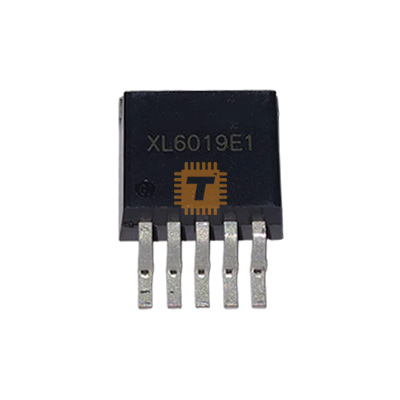
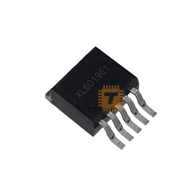
| Name | Original XL6019E1 Boost DC-DC Converter IC TO-263-5L |
| Code | IC0346 |
| Price | Rs.200.00 |
| In Stock | Yes |
| Package | SMD |
Product Details
The XL6019E1 (manufactured by XLSEMI) is a monolithic, high-efficiency Boost (Step-Up) DC-DC converter IC housed in a robust surface-mount TO-263-5L package. Operating at a fixed switching frequency of 180 kHz, this regulator integrates a high-voltage power NMOS switching transistor within the silicon die. This design completely eliminates the need for an external driving transistor, simplifying power system layouts and reducing PCB real estate. It is widely used in power modules to generate stable, higher-voltage output rails from lower-voltage battery or logic supplies.
Specification
- Manufacturer: XLSEMI
- Package Form Factor: TO-263-5L (Surface-mount with 5 pins and a thermal backing tab)
- Topology: Boost (Step-Up) / Flyback / SEPIC Architecture
- Input Operating Voltage Range (VIN): 5V to 40V
- Output Voltage Adjustment Range (VOUT): Up to 60V maximum (Configurable via external resistor divider)
- Maximum Internal Switching Current (ISW): 5A
- Fixed Switching Frequency: 180 kHz (± 20%)
- Feedback Reference Voltage (VFB): 1.25V (± 2?curacy)
- Internal Power NMOS RDS(ON): approx 110 mΩ
- Maximum Duty Cycle: 90%
- Conversion Efficiency: Up to 94% (under optimized load conditions)
- Safety Protections: Built-in Over-Current Protection (OCP), Thermal Shutdown, and Under-Voltage Lockout (UVLO)
Features
- High 5A Internal Current Limit: Equipped with an internal 5A power switch, enabling the chip to handle heavy inductive switching loads without requiring external MOSFET drivers.
- Wide Input Supply Range: Operates seamlessly anywhere from a low 5V supply up to a high 40V rail. This versatility makes it ideal for running off lithium battery packs, 12V automotive systems, or 24V industrial power lines.
- Integrated Frequency Compensation: The chip features internal frequency and loop-stabilization components. This minimizes the need for external filtering networks, simplifying circuit tuning.
- Dedicated TTL Enable (EN) Pin: The
ENpin accepts logic-level signals. Pulling this pin low shuts the regulator down entirely, forcing it into a ultra-low sleep state that draws under 100 μA to preserve power in battery networks.
Common Applications
- Adjustable Boost Power Modules: Serving as the primary controller for high-power, step-up multi-purpose power bank adapters.
- Automotive Electronics Supply: Stepping up fluctuating 12V car batteries to a stable 19V or 24V rail to power accessories, small screens, and mobile computing gear.
- Industrial Telemetry Systems: Boosting standard 5V or 12V instrumentation lines to higher voltages (24V or 36V) required by heavy-duty sensors, actuator loops, and relays.
- Battery-Powered Equipment: Converting low-voltage multi-cell battery packs into higher system operational rails for portable tools and DIY electronics projects.
Professional Usage & Deployment Tips
- Select a High-Saturation Boost Inductor: In a boost topology, the inductor must withstand the peak input switching current, which is significantly higher than the average output load current. Since the XL6019E1 limits internal switching current at 5A, select a power inductor (typically 33 μH to 47 μH) with a physical saturation current (Isat) rating of at least 5.5A to 6A. Using an undersized inductor will cause the core to saturate, triggering overheating, efficiency loss, and voltage ripples.
- Choose the Right Feedback Resistors: The output voltage is set using a resistor divider (R1 from VOUT to FB, and R2 from FB to GND). Calculate the target values using the formula:
VOUT = 1.25V x (1 + (R1/R2)
Keep R2 value between 1 kΩ 10 kΩ to reduce noise sensitivity on the high-impedance
FBpin. - Deploy a High-Speed Schottky Diode: The catch diode bridging the
SWnode to the output filter capacitor must be a high-speed Schottky diode with a rapid reverse recovery time. It should be rated for a continuous forward current of at least 5A and a reverse voltage rating safely exceeding the maximum output target. Never use standard silicon rectifier diodes (like the 1N4007 or 1N5408 series), as they are too slow and will quickly burn out due to excessive switching losses. - Optimize PCB Thermal Real Estate: The TO-263-5L package dissipates heat primarily through its large back tab (Pin 3 / SW node). Solder this tab down to a broad, unbroken copper pour zone on your board. For multi-layer layouts, stitch the copper zone to underlying planes using multiple thermal vias. Without adequate heat dissipation, the IC will rapidly hit its thermal protection boundary (125℃), causing it to shut down or exhibit severe voltage drops.
Sharing is caring, show love and share the product with your friends.
Featured


Add to Cart

Add to Cart

Add to Cart