Original FGH50T65 650V 100A IGBT TO-247 (DI0316) Products
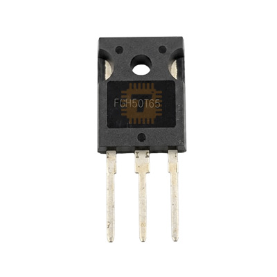
| Name | Original FGH50T65 650V 100A IGBT TO-247 |
| Code | DI0316 |
| Price | Rs.1,260.00 |
| In Stock | Yes |
| Package | TO-220 |
Product Details
The Original FGH50T65 / FGH50T65SQD 650V 100A Field Stop Trench IGBT (TO-247) is a high-speed, high-efficiency insulated gate bipolar transistor engineered for high-power switching applications, solar inverters, and industrial motor drives. Utilizing advanced 4th generation Field Stop Trench IGBT technology, it combines the high input impedance and simple gate drive characteristics of a power MOSFET with the ultra-low on-state conduction loss and high current density of a bipolar transistor. Rated for a collector-emitter breakdown voltage of 650V and a continuous collector current of up to 100A (at Tc = 25°C) / 50A (at Tc = 100°C), it features an ultra-low saturation voltage (VCE(sat) typ. 1.6V), an integrated co-packaged soft-recovery fast anti-parallel freewheeling diode, and a high maximum junction operating temperature of +175°C. Housed in a heavy-duty through-hole TO-247 package, the FGH50T65 is widely utilized in high-frequency arc welding machines, solar PV string inverters, uninterruptible power supplies (UPS), induction heating, active Power Factor Correction (PFC), and high-voltage DC-DC converters.
Specifications
- Part Number / Series: FGH50T65 / FGH50T65SQD Series (Gen 4 Field Stop Trench IGBT)
- Semiconductor Technology: Field Stop 4th Generation Trench IGBT with Co-Packaged Fast Recovery Diode
- Package Type: TO-247-3L / TO-247-3LD (Through-Hole Power Package with Metal Backing Tab)
- Collector-Emitter Voltage (VCES): 650 V (at VGE = 0V, IC = 1mA)
- Gate-Emitter Voltage (VGES): ±20 V (Transient peak rating up to ±30 V)
- Continuous Collector Current (IC):
- At TC = 25°C: 100 A
- At TC = 100°C: 50 A
- Pulsed Collector Current (ICM / ILM): 200 A (TC = 25°C, pulse width limited by max Tj)
- Diode Continuous Forward Current (IF):
- At TC = 25°C: 50 A
- At TC = 100°C: 30 A
- Diode Pulsed Maximum Forward Current (IFM): 200 A
- Collector-Emitter Saturation Voltage (VCE(sat)):
- Typ. 1.60 V (Max. 2.10 V at IC = 50A, VGE = 15V, TC = 25°C)
- Typ. 1.92 V (at IC = 50A, VGE = 15V, TC = 175°C)
- Gate Threshold Voltage (VGE(th)): 2.6 V to 6.4 V (Typ. 4.5 V at IC = 50mA, VCE = VGE)
- Diode Forward Voltage Drop (VF / VFM): Typ. 2.0 V to 2.2 V (Max. 2.6 V at IF = 30A, TC = 25°C)
- Total Power Dissipation (PD):
- At TC = 25°C: 268 W
- At TC = 100°C: 134 W
- Total Gate Charge (Qg): Typ. 99 nC to 102 nC (at VCE = 400V, IC = 50A, VGE = 15V)
- Input Capacitance (Cies): Typ. 3275 pF (at VCE = 30V, VGE = 0V, f = 1MHz)
- Output Capacitance (Coes): Typ. 84 pF
- Reverse Transfer Capacitance (Cres): Typ. 12 pF
- Switching Speed (Inductive Load @ 25°C, VCC = 400V, IC = 25A, RG = 4.7Ω):
- Turn-On Delay Time (td(on)): Typ. 19 ns
- Rise Time (tr): Typ. 13 ns
- Turn-Off Delay Time (td(off)): Typ. 93 ns
- Fall Time (tf): Typ. 6.4 ns
- Total Switching Loss (Ets): Typ. 498 µJ (at 25°C) / 844 µJ (at 175°C)
- Thermal Resistance (Junction-to-Case IGBT, RθJC): 0.56 °C/W
- Thermal Resistance (Junction-to-Case Diode, RθJC): 1.25 °C/W
- Thermal Resistance (Junction-to-Ambient, RθJA): 40 °C/W
- Operating Junction & Storage Temperature (Tj, Tstg): -55°C to +175°C
- Pinout Configuration (TO-247 - Front Printed View, Pins Facing Down):
- Pin 1: Gate (G) - Control Terminal
- Pin 2: Collector (C) - Connected internally to Metal Backing Tab / Flange
- Pin 3: Emitter (E) - Power Return Reference Terminal
- Mounting Flange: Collector (C)
Features
- High-Speed 4th Generation Field Stop Technology: Optimized for medium-to-high switching frequencies (20 kHz to 80+ kHz) with minimal tail current and low total switching energy loss (Ets).
- Ultra-Low Saturation Voltage (VCE(sat) = 1.6V typ.): Minimizes thermal generation and on-state conduction losses during continuous high-amperage operation.
- Positive Temperature Coefficient: VCE(sat) increases slightly with temperature, allowing natural current sharing and easy parallel operation for high-power inverter legs.
- Integrated Fast Anti-Parallel Freewheeling Diode: Soft-recovery characteristics reduce reverse-recovery current spikes and voltage ringing during inductive load commutation.
- 175°C Maximum Junction Operating Temperature: Provides enhanced thermal headroom, robustness, and reliability under heavy industrial and welding duty cycles.
- Rugged TO-247 Package: Large copper baseplate provides low thermal resistance (0.56°C/W) for direct heatsink clamping in forced-air or liquid-cooled power stages.
Common Applications
- Inverter Arc Welding Machines: Primary high-frequency H-bridge and half-bridge switching stages in MMA, TIG, and MIG welding inverters.
- Solar PV String Inverters: DC-AC grid-tied and off-grid high-voltage power conversion and MPPT booster stages.
- Uninterruptible Power Supplies (UPS): High-efficiency DC-AC online double-conversion inverters and battery backup stages.
- Active Power Factor Correction (PFC): High-voltage boost PFC stages in high-wattage power supplies and telecom rectifiers.
- Induction Heating & Cooktops: Resonant half-bridge / full-bridge power oscillator stages for metal forging and domestic induction cooktops.
- Variable Frequency Drives (VFD) & Motor Inverters: 3-phase industrial AC motor speed controllers and electric vehicle auxiliary drive systems.
Usage Tips
- Gate Drive Voltage (VGE): To achieve the specified low saturation voltage (VCE(sat) ≈ 1.6V), drive the gate with a **regulated +15V DC gate voltage**. In high-frequency bridge circuits, use a negative turn-off bias (e.g., **+15V / -5V to -8V**) to prevent parasitic turn-on induced by high dV/dt (Miller effect).
- Dedicated High-Current Gate Driver: Due to the high switching speed and input capacitance, drive the IGBT using a dedicated isolated gate driver IC (such as the **TLP250, HCPL-3120, UCC21520, or IR2110**) with a peak gate sink/source current rating of at least **2A to 4A**.
- Gate Resistor Sizing: Use a series gate resistor (RG) typically between **4.7Ω and 15Ω**. Always place a **10kΩ pull-down resistor** directly across the Gate and Emitter terminals right at the package pins to ensure the IGBT remains safely off during control circuit boot-up.
- Thermal Heatsink & Electrical Isolation: The central metal tab is **internally tied to the Collector (Pin 2)** and operates at high DC link voltages (up to 400V–600V). If mounting multiple devices on a shared grounded heatsink, use high-thermal-conductivity ceramic (Alumina/AlN) or mica insulating pads with insulating shoulder washers and high-performance thermal grease.
- High-Frequency DC Bus Snubbing: To protect against inductive turn-off overvoltage spikes, place low-ESR polypropylene film snubber capacitors (e.g., 0.1µF to 0.47µF, 630V/1000V) as close as possible across the primary high-voltage DC bus supply rails (+DC and -DC/GND) right at the IGBT collector-emitter nodes.
Sharing is caring, show love and share the product with your friends.
Featured

Add to Cart


Add to Cart

Other Products

Add to Cart